
Finished NO SCHOOL ! Here are some things I learned regarding the board itself :
- the low profile VGA connector is a nightmare, never again.
- the reset button needs to go elsewhere as Lattice IceCube doesn’t like pin 66 for some reason
- the 3D printed cases suck, not necessary and doesn’t have NO SCHOOL on it
- the pads for the bias trim knob kept breaking, not sure if it is bad PCB manufacturing or poor design. Also a bit too hard for beginners to solder this part.
- the portable low power soldering irons sucked for this
- I can remove the caps and 1K resistors for the button debouncing
- the video pass through mode is annoying to set up (needing an audio cable, remembering which pin is H and V sync etc.)
- People like the mechanical keys
- The VCC and GND is useful for powering a breadboard with other video mods
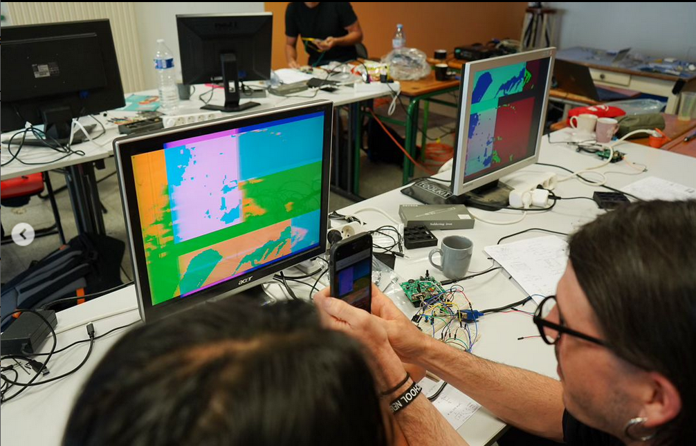
Regarding the hands on video glitching workshop :
- Breadboards and pinout of the VGA connector tough to get the hang of.
- Important to make a safe space – you can’t hurt yourself, nothing valuable here, etc.
- I did a free-style open-ended workshop but still ended up starting with asking the participants to :
- use jumpers to plug in their board to a VGA cable (though I should have skipped this and went directly to plugging in to the breadboard)
- use jumpers to plug in their board to a breadboard and then to the VGA cable
- use switches to turn on or off different channels
- use pots to attenuate different color channels
- use coil of wire to make a delay
- use LM386 to amplify
- 74*04 to invert
- Circuit bending the schmitt trigger
- Mixing signals: 74*86 to XOR, or just pots
- I should have gotten them to put audio in the pass through mode !
- Forgot to ask them to make BLACK AND WHITE from color
- There was no oscilloscope or function generator to work with, I should have brought a logic analyzer too
- Karl Marx was a big hit
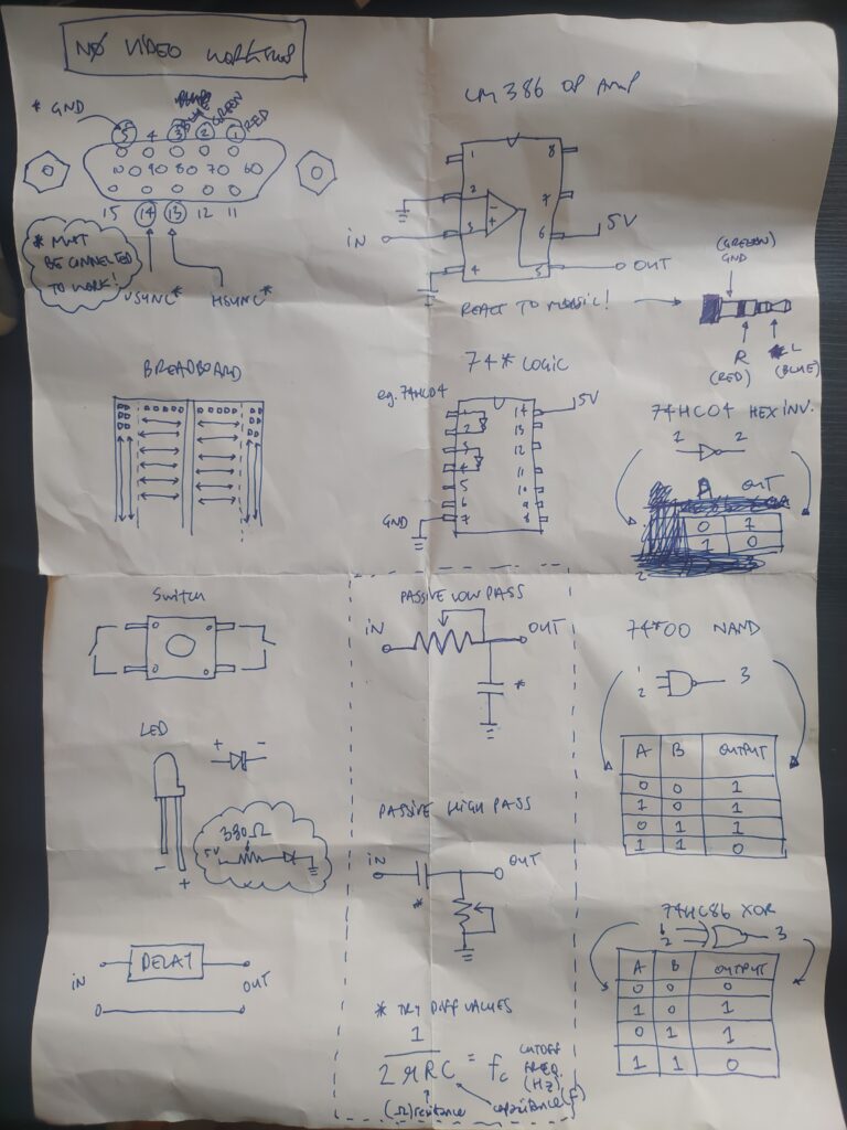
- I hand drew some schematics (pinouts of various chips, circuits etc.) and printed them, then would project and draw on the big board the pinouts
- They have difficulty with the translation of schematic to actual connections.
- I can imagine a board made specifically for this workshop which would have an FPGA or Arduino (but without any buttons just as a kind of screen saver) and would connect to a breadboard, breaking out the different pins, where you could do things. This would have gotten around the pain of plugging in jumpers to the VGA connectors, and would be far less work than making the entire FPGA béchamel board. It could be a super basic atmega with just a knob to select patterns.
****
Paul suggests adding to my open source FPGA video synth page :
- A nicer README that explains the project in depth and uses Markdown to make things easier and nicer to read and navigate
- An explanation of how people can use and contribute to the project
- A better organization of the files in the project
- Selecting a licence
- Using git on the PC instead of Github
I really like the idea of doing a super page with gifs explaining what codes do, compiled binaries and commented verilog codes.
I wonder if I could work on a series of separate effects, each with it’s own module, that would allow people to add effects.
Looking in to open source hardware projects for inspiration:
- OPEN MV (https://github.com/openmv/openmv): Uses an 32-bit Arm Cortex-M4 chip with DSPs.
- MUTABLE INSTRUMENTS (https://pichenettes.github.io/mutable-instruments-documentation/) Open source versions of classic eurorack modules
I have rebuilt the git repo and it looks way better now :
What I’ve learned :
- I can import Eagle boards (but not my schematics so far) into KiCAD but I should build using KiCAD from now on for open source projects
- I can take all the energy I was using to make this website and put it into making an awesome README for my project
- A project can almost start with the README, so that it is clear from the beginning what the thing is and what it does
I’ve also promised to send boards to people, perhaps a little prematurely ! Ideally it would be easy for people to upgrade their firmware, this way I could freeze the hardware design and just focus on making code. But this would require giving them a programmer ?
******
Check out this FPGA graphics tutorial : https://projectf.io/posts/fpga-graphics/
Essentially, start by generating a pixel clock for the chosen resolution. Look up standard VGA timings and set up the parameters for blanking etc. Set up a counter and a display enable signal, and then create shapes by using equality operators and colors.
This racing the beam tutorial (https://tomverbeure.github.io/rtl/2018/11/26/Racing-the-Beam-Ray-Tracer.html) explains that if you don’t have enough space for a frame buffer you can have a line buffer, or even a pixel buffer, if you can compute things fast enough. Later in the series using raster font in a simple way, sprites in ROM and scaling them, and creating a simple color LUT.
The screen buffer article is informative : https://projectf.io/posts/framebuffers/ . Especially how to scale up 160×120 framebuffer up to 640×480. Also this one on the three different strategies for making FPGA animations : https://projectf.io/posts/animated-shapes/
This looks like a good FPGA tutorial resource I wasn’t aware of:
- http://asic-world.com/verilog/index.html
- https://projectf.io/tutorials/
- http://fpgacpu.ca/fpga/index.html
- https://zipcpu.com/tutorial/
- http://www.doe.carleton.ca/~gallan/478/pdfs/PeterVrlR.pdf
- https://fpgaer.tech/?p=191
To decode HDMI found this : https://warmcat.com/hardware%20design/hdmi/fpga/2015/10/22/hdmi-capture-and-analysis-fpga-project-3.html
**********
I think this project has been a victim of a certain amount of magical thinking. The machine will only do what it can do and what it is asked to do. Yes, it’s possible to glitch the machine but ultimately there are no surprises unless you don’t fully understand what you’re asking the machine to do. It’s all deterministic. Learning the history of graphics is super cool but you are just reproducing old techniques, there isn’t going to be some hidden type of graphic expression that was missed by everyone that you are going to unlock somehow. It’s just colors on a screen in the end…
It’s ultimately an activity I enjoy, and it is best to share things you enjoy with other people. I should connect with other people making things !
*****
Here’s the final pcf :
// CLOCK

set_io clk_in 49

// HDMI OUT

set_io hdmi_p[0] 139 -io_std SB_LVCMOS
set_io hdmi_p[2] 78 -io_std SB_LVCMOS
set_io hdmi_p[1] 80 -io_std SB_LVCMOS
set_io hdmi_p[3] 137 -io_std SB_LVCMOS

set_io hdmi_n[0] 138 -io_std SB_LVCMOS
set_io hdmi_n[2] 79 -io_std SB_LVCMOS
set_io hdmi_n[1] 81 -io_std SB_LVCMOS
set_io hdmi_n[3] 136 -io_std SB_LVCMOS

// VGA OUT

set_io v_sync 97
set_io h_sync 76

set_io r_out[0] 91
set_io r_out[1] 95
set_io r_out[2] 96

set_io g_out[0] 75
set_io g_out[1] 74
set_io g_out[2] 73

set_io b_out[0] 87
set_io b_out[1] 88
set_io b_out[2] 90

// SOUND OR VGA ANALOG IN

set_io analog_in 56

// POTENTIOMETER IN

set_io pot_in 52

// KEYS IN

set_io key[0] 37
set_io key[1] 38
set_io key[2] 39
set_io key[3] 41
set_io key[4] 42
set_io key[5] 43
set_io key[6] 44
set_io key[7] 45
set_io key[8] 47

// LEDS OUT

set_io green_led 23
set_io red_led 24

// VGA IN

set_io rpi_hsync 34
set_io rpi_vsync 31
I am working on a demo code that brings everything together : sound in, pot in, button reactivity, random, sine, time, VGA (and maybe HDMI?). Here is what it looks like so far :
module vga_sync_test(
input wire clk_in,
input wire [8:0] key,
input wire rpi_vsync,
input wire rpi_hsync,
input wire analog_in,
inout pot_in,
output [3:0] hdmi_p,
output [3:0] hdmi_n,
output reg [3:0] r_out,
output reg [3:0] b_out,
output reg [3:0] g_out,
output wire h_sync,
output wire v_sync,
output wire red_led,
output wire green_led
);

wire display_en;
//reg [9:0] h_count;
wire [11:0] h_count;
//reg [9:0] v_count;
wire [11:0] v_count;

localparam h_pixel_max = 1280;
localparam v_pixel_max = 960;
localparam h_pixel_half = 640;
localparam v_pixel_half = 480;


reg [4:0] addr;
reg [7:0] data;
reg [7:0] data_out;
always@(addr) begin
case (addr)

0 : data = 0;
1 : data = 16;
2 : data = 31;
3 : data = 45;
4 : data = 58;
5 : data = 67;
6 : data = 74;
7 : data = 77;
8 : data = 77;
9 : data = 74;
10 : data = 67;
11 : data = 58;
12 : data = 45;
13 : data = 31;
14 : data = 16;
15 : data = 0;
16 : data = -16;
17 : data = -31;
18 : data = -45;
19 : data = -58;
20 : data = -67;
21 : data = -74;
22 : data = -77;
23 : data = -77;
24 : data = -74;
25 : data = -67;
26 : data = -58;
27 : data = -45;
28 : data = -31;
29 : data = -16;
default : data = 0;
endcase
end

reg[22:0] div_cntr1;
reg[22:0] div_cntr2;
reg half_sec_pulse;

always@(posedge clk_in)
begin
div_cntr1 <= div_cntr1 + 1;
if (div_cntr1 == 0)
if (div_cntr2 == 0)
begin
div_cntr2 <= 0;
half_sec_pulse <= 1;
end
else
div_cntr2 <= div_cntr2 + 1;
else
half_sec_pulse <= 0;

end


always @(posedge half_sec_pulse) begin

data_out <= data;
addr <= addr + 1;
if(addr == 29)
addr <= 0;

end

// FOR AUDIO IN INTERACTION
assign red_led = analog_in;
assign green_led = analog_in;

// FOR KEY INTERACTION key[8:0]

// FOR POT INTERACTION

reg [15:0] adc_count= 0; //16 bits to count how long it's taking to charge. 32,768 is the max value. 1 extra MSB bit for just discharging the cap.
reg [14:0] pot_value= 0; //to store cap charge time value
reg [14:0] final_pot_value= 0;

wire adc_in;
reg adc_sample = 1; //first time through we want to sample the cap value

wire adc;


assign pot_in = (adc_sample) ? 1'bZ : 1'b0;
assign adc_in = pot_in;

// for a 25MHz clock we divide 100MHz by 4
reg [1:0] clk_div = 0;

always @(posedge clk_in)
begin
clk_div <= clk_div + 1;
end


always @(posedge clk_div[1]) begin //25MHz clock

adc_count <= adc_count + 1; // start counting

if(adc_count>=16'b1000000000000000 )begin // once we have rolled over 15 bit counter...

adc_sample <= 1'b0; // ...discharge cap for a while to restart the process.

end

else begin

adc_sample<=1'b1; //put cap pin in high 'Z'

if(adc_in==1'b1) begin // if cap charged...

pot_value[14:0]<=adc_count[14:0]; //store this value in pot


end

end

end


// FOR SOUND INTERACTION

// FOR AUDIO IN INTERACTION

//Check if we can create RGB colors
always @(posedge clk_in) begin


if (display_en) begin
if (h_count < h_pixel_half + data_out
&& v_count < v_pixel_half - data_out) begin
//Assign here your test color


//pot changing colors
case(pot_value[14:13])

2'b00: begin //yellow
r_out <= 3'b010;
g_out <= 3'b110;
b_out <= 3'b011;
end
2'b01: begin //cyan
r_out <= 3'b011;
g_out <= 3'b100;
b_out <= 3'b001;
end
2'b10: begin //magenta
r_out <= 3'b110;
g_out <= 3'b110;
b_out <= 3'b011;
end
2'b11: begin //blue
r_out <= 3'b010;
g_out <= 3'b111;
b_out <= 3'b111;
end

default: begin // white
r_out <= 3'b010;
g_out <= 3'b010;
b_out <= 3'b011;
end
endcase


end else if (h_count > h_pixel_half - data_out
&& v_count < v_pixel_half + data_out) begin

if (analog_in == 1) begin
//Assign here your test color
r_out <= 3'b010;
g_out <= 3'b110;
b_out <= 3'b011;
end
else begin
r_out <= 3'b001;
g_out <= 3'b010;
b_out <= 3'b100;
end
end else if (h_count < h_pixel_half - data_out
&& v_count > v_pixel_half - data_out) begin
//Assign here your test color
r_out <= key[2:0];
g_out <= key[5:3];
b_out <= key[8:6];
end else begin
//Assign here your test color
r_out <= 3'b010;
g_out <= 3'b010;
b_out <= 3'b010;
end
end else begin
r_out <= 3'b000;
g_out <= 3'b000;
b_out <= 3'b000;
end
end

vga_sync vga_s(
.clk_in(clk_in), //12MHz clock input
.h_sync(h_sync),
.v_sync(v_sync),
.h_count(h_count),
.v_count(v_count),
.display_en(display_en) // '1' => pixel region
);

endmodule
**************
What is next ?
I am tasked with making an installation using a camera and the FPGA to demonstrate its ability to modify an incoming video stream. I’m going with this simple OV7670 Camera. I would also like to have something to mail to my new video and audio synthesis contacts in Lyon.
I have displayed an image saved in ROM, but I would also like to sample a 120×160 pixel image into BRAM from an incoming video stream. (If this is not possible, I’lll use the SRAM on the Cyber Campus board.)
I’m planning on starting this process with an RPI set to output 60Hz 640 x 480 (https://pimylifeup.com/raspberry-pi-screen-resolution/) and use an HDMI to VGA converter to send this along to the FPGA.
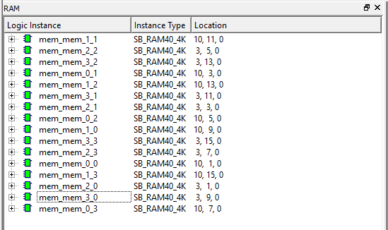
I can access all 16 x 4k BRAMS now :
module ram (din, write_en, waddr, wclk, raddr, rclk, dout);// 32768 x 2
parameter addr_width = 15; // to access all 32768 bits of the address
parameter data_width = 2;
input [addr_width-1:0] waddr, raddr;
input [data_width-1:0] din;
input write_en, wclk, rclk;
output reg [data_width-1:0] dout;
reg [data_width-1:0] mem [(1<<addr_width)-1:0]
;
always @(posedge wclk) // Write memory.
begin
if (write_en)
begin
mem[waddr] <= din; // Using write address bus.
end
end
always @(posedge rclk) // Read memory.
begin
dout <= mem[raddr]; // Using read address bus.
end
endmoduleBut so far once I start using it, it disappears ! Moving back to SRAM.
It’s working really nicely taking the 160×120 ROM image and using it as a screen buffer.
addr <= (((hc-hbp)>>2)+(((vc-vbp)>>2)*160));Here’s the input from this pattern :
assign data_in[7:0] = (again_xnor[7:0] > key[7:0]) ? 8'b11111111 : 8'b00000000;
And here is the recording which stays nice and still !

The horizontal lines appeared when I moved away from
this :

if ((rec==0) && (a>=8'b10000000))

to this :
if ((rec==0) && (a==8'b00000000))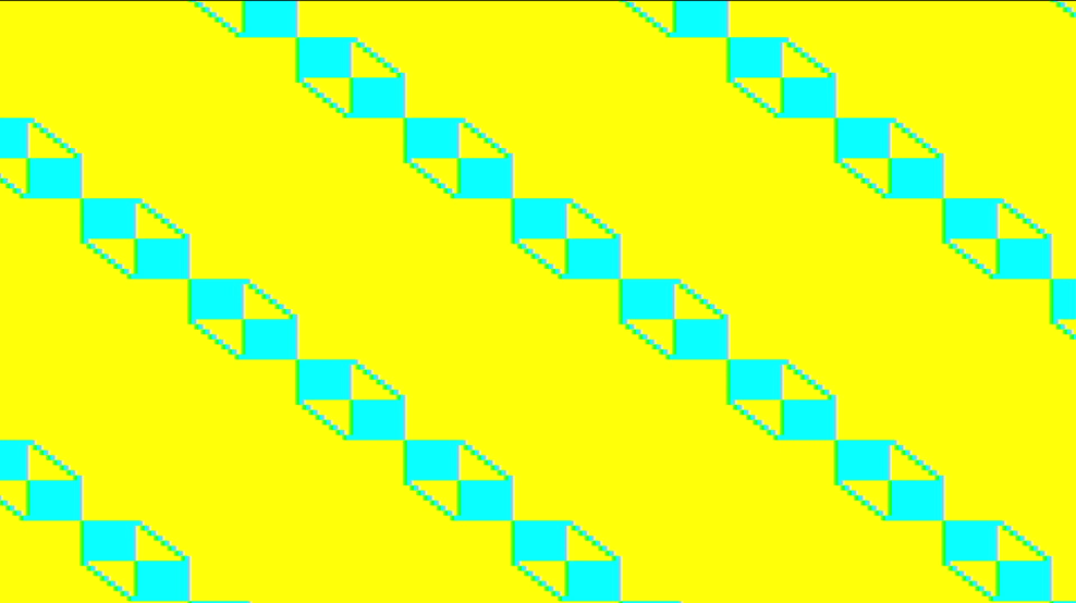

I am trying to record incoming VGA color but then I remembered the HDMI clock is 25MHz and the VGA is 50 MHz (?). I can solder the VGA connector to the SRAM version of the board and switch to VGA, or I could modify the vga.sync of the input VGA board to run at 25MHz with standard 640×480 using a PLL.
I could also now try some framebuffer animations !
I can now output standard 25MHz 640×480 VGA. I changed vga_sync to have 640×480 timings by selecting these parameters :
localparam h_pixel_total = 800;
localparam h_pixel_display = 640;
localparam h_pixel_front_porch_amount = 16;
localparam h_pixel_sync_amount = 96;
localparam h_pixel_back_porch_amount = 48;

localparam v_pixel_total = 525;
localparam v_pixel_display = 480;
localparam v_pixel_front_porch_amount = 10;
localparam v_pixel_sync_amount = 2;
localparam v_pixel_back_porch_amount = 33;
And then changing the values in the verilog file making graphics :
localparam h_pixel_max = 640;
localparam v_pixel_max = 480;
localparam h_pixel_half = 320;
localparam v_pixel_half = 240;

...


// for a 25MHz clock we divide the 100MHz clk_in by 4
reg [1:0] clk_div = 0;

always @(posedge clk_in)
begin
clk_div <= clk_div + 1;
end
...

vga_sync vga_s(
.clk_in(clk_div[1]), // giving vga_sync the 25MHz clock
.h_sync(h_sync),
.v_sync(v_sync),
.h_count(h_count),
.v_count(v_count),
.display_en(display_en) // '1' => pixel region
);

endmodule
*****
I can now record relatively stable VGA, it still appears to drift a little though (doesn’t help to use test if HSYNC high). Will need to try with rpi in 640×480 mode. From now on I want to use standard timings for all the rpi video out, the VGA and HDMI timings for the FPGAs so that transitioning is as painless as possible. I’ll try with the rpi in 25MHz mode later today.
I want to try changing the size of the screen buffer, and eventually recording video by moving the buffer deeper into SRAM memory over time. Success ! I just divided the horizontal and vertical counters by 2 instead of 4 and increased the horizontal line width from 160 bits to 320.
addr <= (((hc-hbp)>>1)+(((vc-vbp)>>1)*320));
320 x 240 (76,800 pixels) screen buffer !! I have a total of 256,000 I could use.

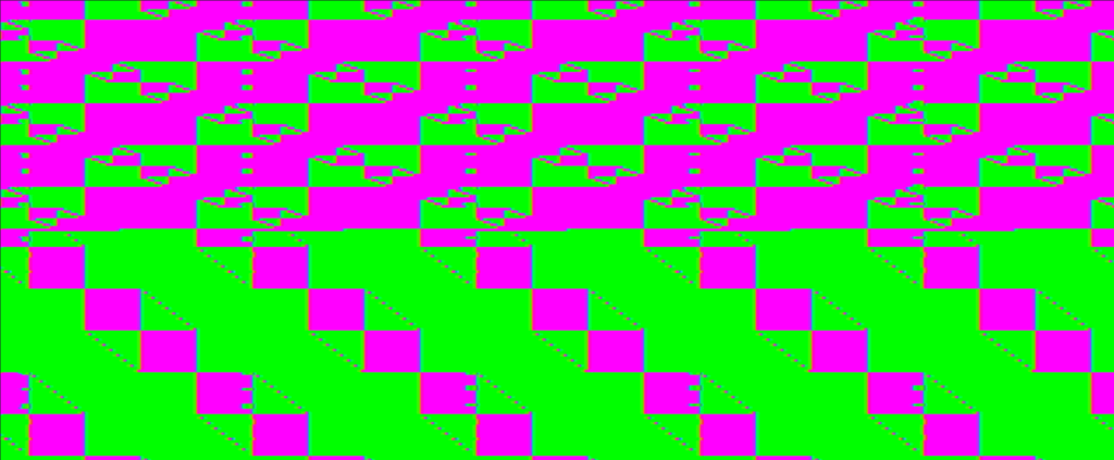
Much finer tune recording possible (despite the added noise)

I am trying to record 3 frames but it’s making extra glitchy things happen (most important stuff bold) :
...
else
begin
hc <= 0;
if (vc < vlines) begin
vc <= vc + 1;
screen_count <= screen_count + 1;
end
else
vc <= 0;
end
end
else begin
c0_high_speed <= {2'b00, c0_high_speed[9:2]};
c1_high_speed <= {2'b00, c1_high_speed[9:2]};
c2_high_speed <= {2'b00, c2_high_speed[9:2]};
clk_high_speed <= {2'b00, clk_high_speed[9:2]};
latch_high_speed <= latch_high_speed + 1'b1;
end
end

always @(posedge latch_high_speed[2]) // display 100% saturation colourbars
begin

case(screen_count[9])

1'b0 : multiplier = 1;
1'b1 : multiplier = 2;

default : multiplier = 1;

endcase

// first check if we're within vertical active video range
if (vc >= vbp && vc < vfp)
begin
// now display different colours every 80 pixels
// while we're within the active horizontal range
// -----------------
if(hc >= hbp && hc < hfp) begin

//pixel <= heart[(((hc-hbp)>>2)+(((vc-vbp)>>2)*160))];
addr <= (((hc-hbp)>>1)+(((vc-vbp)>>1)*320*multiplier));

...
In theory though this would be useful for double buffering.
I am trying to record in three different parts of the SRAM based on the key pressed.
...

case(key[7:6])
2'b00: multiplier = 1;
2'b01: multiplier = 2;
2'b10: multiplier = 3;
2'b11: multiplier = 1;

default: multiplier = 1;
endcase

if (vc >= vbp && vc < vfp)
begin

if(hc >= hbp && hc < hfp) begin

addr <= (((hc-hbp)>>1)+(((vc-vbp)>>1)*320*multiplier));

...
They seem to be partially overwriting one another however :
SOLVED : Needed to add an offset which was higher than the highest memory location that could be reached in the first screen buffer (78,000). I have a total of 256,000 so I could save a few more images.
...

case(key[7])
2'b0: offset = 0;
2'b1: offset = 78000;
default: offset = 0;
endcase


if (vc >= vbp && vc < vfp)
begin

if(hc >= hbp && hc < hfp) begin

addr <= (((hc-hbp)>>1)+(((vc-vbp)>>1)*320)+ offset);

...
Going to try an animation but using the smaller 160×120 sized buffer.
SUCCESS ! I incremented screen_count every 600 frames :
if (vc < vlines) begin
vc <= vc + 1;
frame <= frame + 1;
if(screen_count>12)begin
screen_count <= 0;
end
if (frame > 6000) begin
screen_count <= screen_count + 1;
frame <= 0;
end
end

...

addr <= (((hc-hbp)>>2)+(((vc-vbp)>>2)*160)+(offset*screen_count));
*****
The three ways I could start doing cool stuff with this screen buffer (from https://projectf.io/posts/animated-shapes/):
- Use hardware sprites – suitable for simple 2D graphics
- Use a blitter to cut out and move a framebuffer region – effective for small 2D objects
- Clear the framebuffer and draw from scratch – versatile but requires plenty of bandwidth
Animations might start to reveal the limitations of the (non dual ported) SRAM. The website suggests either using the blanking space to update SRAM or double buffering with a finite state machine to switch and clear them. I could use the FPGA internal memory for ROM storage of colour look up tables, sprites and textures?
I want to try overlaying text from ROM onto the screen, to have a splash screen when the FPGA powers up.
****
To solve the setting of the top_module, I think I have a solution (untested so far):
- In iCECube 2, right click on Run Synplify Pro Synthesis and select options
- Under tool options, click on To set Synplify Pro option, click here
- A new Synplify Pro window opens up
- Select the Design Hierarchy tab to set the top module
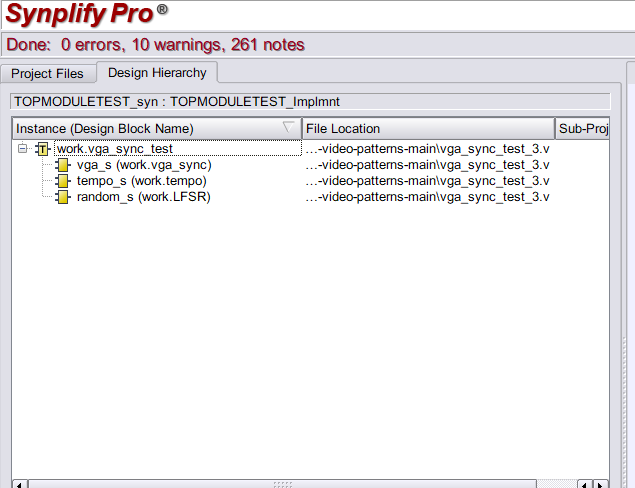
- Now click RUN and close the Synplify Pro window afterwards
- iCECube2 Should now have green ticks next to Run Synplify Pro Synthesis and Select Implementation
- Finish the process by executing the remaining steps not yet checked in green
Some learningz reading a french magazine for beginner engineers :
To find out how many bits are required to store a max number, you take the log base 2 of a number, and round up to the nearest integer.
ceiling of log₂(12000000) = 23.51, we round up to get 24 bits needed to store the 12,000,000 decimal number.
If we want to know what the final frequency of an LED blinking will be with a given counter and clock speed :
(2^24 -1) / 12MHz = 1.4Hz = blink frequency (if toggling every roll over of a 24 bit register with a 12MHz clock)
Also learned about linting, the process of testing a code for suspicious constructs that might have been missed by a compiler : https://projectf.io/posts/verilog-lint-with-verilator/
****
Check out the Poietic Generator :


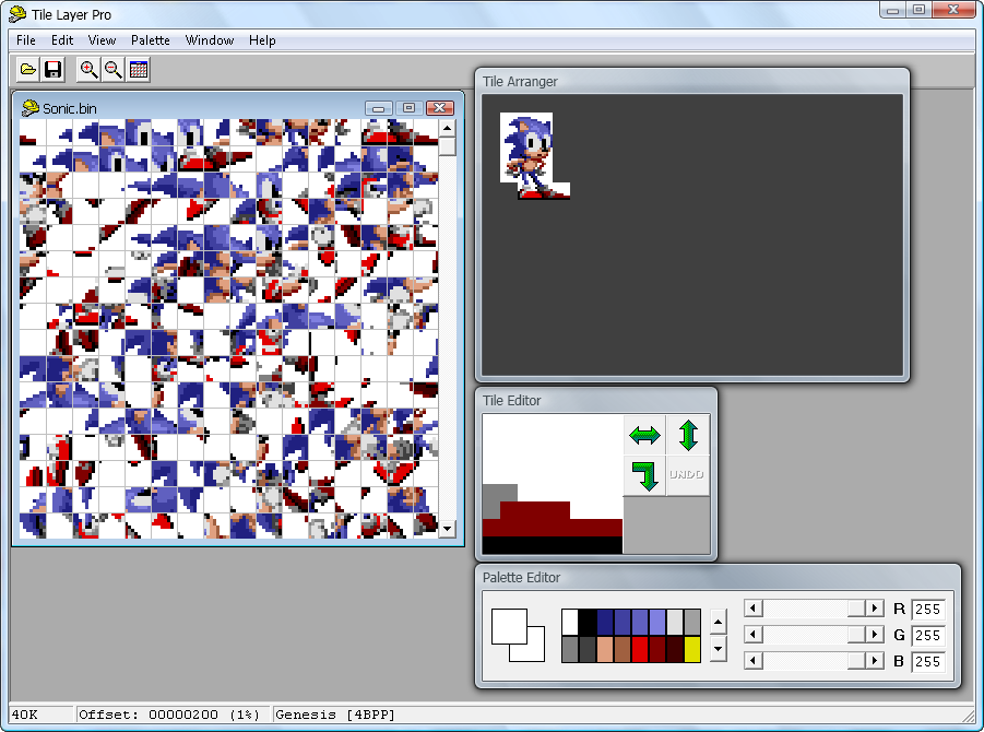
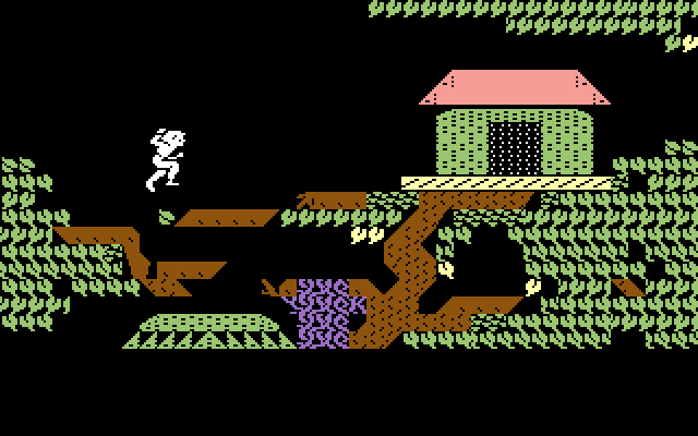
Also Looking at different raster memory editors for games in the 1980s :
![]()


There is also this project Viewpoint that appears to allow the user to edit sprites in real time : https://www.youtube.com/watch?app=desktop&v=9G0r7jL3xl8
There are two programs for looking at RAM while playing NES video games called No$sns and bizhawk. I learned about them from this great series Retro Game Mechanics Explained (https://www.youtube.com/@RGMechEx/videos) Here’s a screen shot :
Some other cool links from a Hacker News deep dive :
https://bost.ocks.org/mike/algorithms/
https://pixel.essenmitsosse.de/?showcase=true&slide=4

https://chrisbuilds.github.io/terminaltexteffects/showroom/
http://web.archive.org/web/20240307215347/http://www.buthowdoitknow.com/but_how_do_it_know_cpu_model.html

Below the root game :
https://obsolescence.wixsite.com/obsolescence/pidp-11

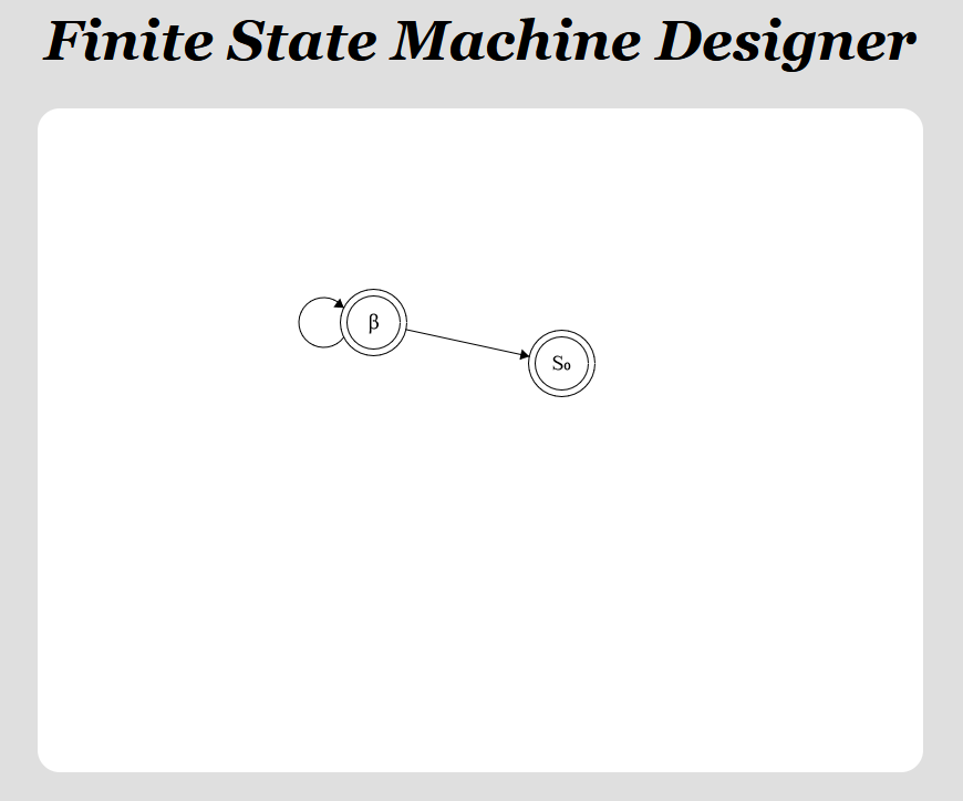
https://madebyevan.com/fsm/
On the SNES graphics systems :
https://fabiensanglard.net/snes_ppus_how/index.html
https://fabiensanglard.net/snes_ppus_why/
On RASTEROPs or BITBLT or bit blitting or Bit Block Transfer:
http://www.leptonica.org/rasterops.html#WHAT-IS
Cool thing from this article is the way in which simple bit shifting and masking operations can do affine transformations like translate, shear, rotate to paint and repaint bitmap images into the framebuffer and analyze images (not sure how though).
The article explains how to shear, rotate and translate between a source and destination image using these simple operations ( and something else about erosion and dillation):
Coding a reverb :
https://signalsmith-audio.co.uk/writing/2021/lets-write-a-reverb/
****
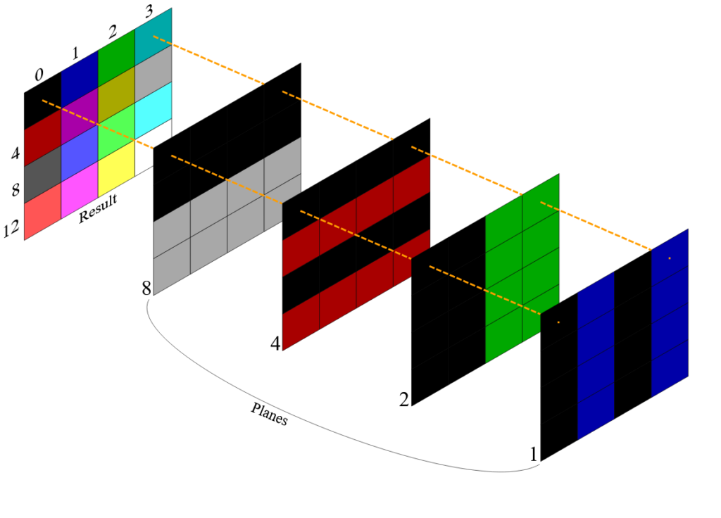
https://upload.wikimedia.org/wikipedia/commons/5/5b/Diagram_of_planar_computer_graphics.svg
Combining different bit planes together to get a final result :
and finally a swap chain buffer system :
https://en.wikipedia.org/wiki/Swap_chain