Thoughts on this as a product now that SD card seems possible :
- I could put “sprites” like the bechamel logo and some numbers in some location in memory.
- I could be able to save screen shots on the SD card with a button combo.
- Could there be a kind of database, which would be like how rhino saves files of 3D models one is working on ?
- Am I making a mini computer (ALU, slow big memory, fast SRAM, user interface, screen output) ? What do I think about a scroll wheel and a mini screen then ?
- What could I do with a stack of images from the SD card ?
Just a reminder of what a fully fleshed out video system looks like with the Gameduino : https://excamera.com/files/gameduino/synth/doc/gen/poster.pdf
*********
Checking-in with my project goals for 2024.
- This year the goal was to have a finished open-source project that could be shared with people online or as a kit/product via prepared instruments.com. I would be able to show it to students as an example of a finished design/engineering project that I have completed. The idea would be to stabilize the design, to stop making endless boards, and begin exploring more verilog codes that run on it.
Currently, the Cyber Campus version of the board is basically complete enough to transition into just trying new code. There is just the SD card that remains before the object has a feel of being an independent finished object that isn’t dependent on any other products (like rpi) to function.
Perhaps a distinction between the product, art and workshop kit would be useful :
Kit : reprogrammable, built around the rpi, solderable by beginners, etc.
Product : HDMI IN (a compromise would be that chip that handles everything like the TFP401PZP) and HDMI OUT, plug and play with modern tech. Has a larger FPGA to be able to do more cool stuff.
Art : The Cyber Campus version has everything I need to have fun with new codes, especially ones that interact with time and sequence (like temporal compression?), like differences between images in time impacting the kinds of transformations instead of staying with just static filters.
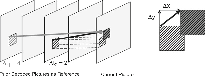
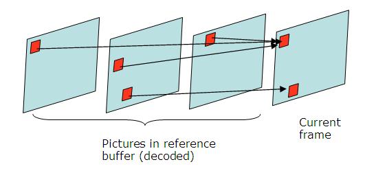
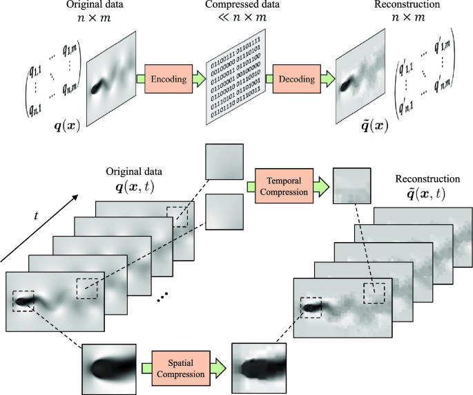
*********
I need to make the SD card code more generalizable with a function that takes CMD IN.
Here is the command format :
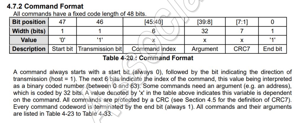
For example CMD8, the first byte is 01001000 with : 0 (start bit) + 1 (tx bit) + 010000 (six bits of the CMD number 8 in binary). After this are 32 bits of arguments (such as address you want to select) the 6 bit CRC7 and then 1.
NOTE ** I may need to change the speed from 50KHz to 100KHz or 200KHz for things to work. I am unclear about when I need to send ticks but forum user writes this :
; There must be 8 clocks after
; * a command with no response
; * the response of a command with a response
; * the end of a read data block
; * the CRC status token on a write
Here is the sequence of commands I have so far :
//TICKS
parameter TICKS = 48'b11111111_11111111_11111111_11111111_11111111_11111111;

//CMD0 “GO_IDLE_STATE”
parameter CMD0 = 48'b01000000_00000000_00000000_00000000_00000000_10010101;

//CMD8 “SEND_IF_COND”
parameter CMD8 = 48'b01001000_00000000_00000000_00000001_10101010_10000111;

//CMD55 “APP_CMD”
parameter CMD55 = 48'b01110111_00000000_00000000_00000000_00000000_01100101;

//ACMD41 “SD_SEND_OP_COND”
parameter ACMD41 = 48'b01101001_01000000_00010000_00000000_00000000_11001101;

//CMD2 “ALL_SEND_CID”
parameter CMD2 = 48'b01000010_00000000_00000000_00000000_00000000_01001101;

//CMD3 “SEND_RELATIVE_ADDR”
parameter CMD3 = 48'b01000011_00000000_00000000_00000000_00000000_00100001;

//CMD7 “SELECT/DESELECT_CARD”
parameter CMD7 = 48'b01000111_00000000_00000000_00000000_00000000_CRC+1; // need to generate my own CRC for this

//CMD17 “READ_SINGLE_BLOCK”
parameter CMD17 = 48'b01010001_00000000_00000000_00000000_00000000_CRC+1;
NOTE ** There is a read multiple block command CMD18 READ_MULTIPLE_BLOCK that takes a 32 bit address and continuously transfers data blocks until interrupted by the STOP_TRANSMISSION command. By default sends 512 bytes followed by a CRC.
I am currently breaking up the code into cycles of 48 clock pulses to send and receive commands in sequence.
counter <= (counter==47) ? 0 : counter+1; // to count the steps in the sending of a single CMD
phase <= (counter==47) ? phase+1: phase; // to count how many CMDs we have sent
Each command is currently sent in order by checking the phase. For example :
if (phase == 8) begin
      rec <= 1; // set CMD to output
      CMD <= ACMD41[counter]; // iterate through the 48 bit command
end
Listening to input is tougher because of my poor understanding of inout, I am using inout to define the CMD pin. If we are receiving it is put in a high Z state.
assign CMD = rec ? CMD : 1'bz;I am not sure if this will work :
if (phase == 9) begin
      rec <= 0; // set CMD inout pin to high Z
      data_in[counter] <= CMD; //store the data in data_in
end
Here I’m trying to check if a ready bit 31 is still unset :
if ((data_in & (1<<31))==0)Here I’m trying to compose the CMD7 by concatenating the appropriate bytes.
//CMD7 “SELECT/DESELECT_CARD”
if (phase == 16) begin
   rec <= 1;
   RCA[15:0] = data_in[31:15]; // retrieve the RCA from the previous response
   CMD7[47:0] = {8'b01000111,RCA[15:0],16'b0000000000000000,CRC+1}; // compose CMD7 from parts
   CMD <= CMD7[counter]; // send the command
end
****
I’m on this site to calculate the CRC7 (https://www.ghsi.de/pages/subpages/Online%20CRC%20Calculation/)
- First I enter the CRC polynomial which for the SD card is x7 +x3 + 1
- Then I translate the 5 bytes I want to send into hex
- The 7 bit value generated at the end of the page is then added to the end of the message plus the end bit (1)
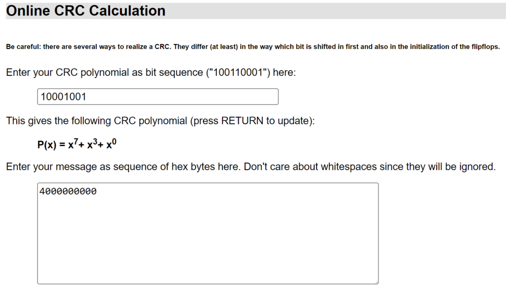
I need to figure out how to incorporate the CRC in verilog for certain commands however :
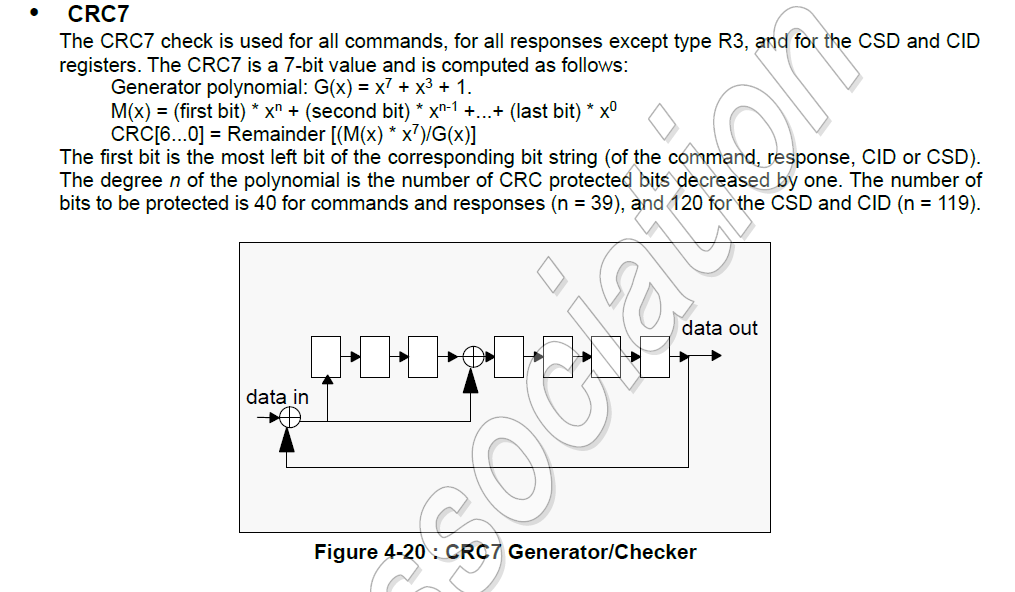
The above website automatically generates this verilog code that takes one bit at a time :
// ==========================================================================
// CRC Generation Unit - Linear Feedback Shift Register implementation
// (c) Kay Gorontzi, GHSi.de, distributed under the terms of LGPL
// ==========================================================================
module CRC_Unit(BITVAL, BITSTRB, CLEAR, CRC);
input BITVAL; // Next input bit
input BITSTRB; // Current bit valid (Clock)
input CLEAR; // Init CRC value
output [6:0] CRC; // Current output CRC value

reg [6:0] CRC; // We need output registers
wire inv;

assign inv = BITVAL ^ CRC[6]; // XOR required?

always @(posedge BITSTRB or posedge CLEAR) begin
if (CLEAR) begin
CRC = 0; // Init before calculation
end
else begin
CRC[6] = CRC[5];
CRC[5] = CRC[4];
CRC[4] = CRC[3];
CRC[3] = CRC[2] ^ inv;
CRC[2] = CRC[1];
CRC[1] = CRC[0];
CRC[0] = inv;
end
end

endmodule
I am not sure exactly how to feed this module one bit at a time. I also feel unsure about how to properly incorporate modules from different files.
****
Here is my test code (once the timescale is uncommented) that I’m hoping will not require CRC (I’ll just look on the oscilloscope to see what the RCA is and then use that). It is the simplest possible setup.
Possible things that need changing :
- I am not waiting to see if bit 31 is set after sending
ACMD41, so I probably will need to add a delay here ? *EDIT* I am getting a busy bit 31 the first time I ask at the moment. - 8 clock ticks instead of 48 ? *EDIT* DONE
- No clock ticks after certain commands?
- The RCA (and CRC) if it is not 0001
- The block address (and CRC) if it is not 0
//-----------------------------------------------------------------
// - Attempt at SD 1 bit communication -
//CMD0 “GO_IDLE_STATE”
//CMD8 “SEND_IF_COND”
//CMD55 “APP_CMD”, ACMD41 “SD_SEND_OP_COND” with argument 40100000 (HCS=1, voltage = 3.3).
//The R3 response has HCS and the supported voltages set. Repeat until bit 31 of the response is 1.
//CMD2 “ALL_SEND_CID” with argument 00000000. The R2 response has the CID. I ignore it.
//CMD3 “SEND_RELATIVE_ADDR” with argument 00000000. The R6 response contains the RCA and some status that I ignore.

//The card is now in the stand-by state. Reading a block is accomplished by
//CMD7 “SELECT/DESELECT_CARD” with argument bits 31-16 = the RCA you were given, 15-0 = 0. The R1b response I ignore.
//CMD17 “READ_SINGLE_BLOCK” with argument = the block address.
//The R1 response I ignore, but there will also be the block data.
//Keep toggling the clock, and you’ll eventually see a start bit followed by a block of data and a CRC.
//-----------------------------------------------------------------

`default_nettype none // disable implicit definitions by Verilog
//`timescale 1us/1ns

module top(
input wire clk100,
input wire reset,
//input reg DAT,
output reg SCK,
output reg CMD
);

//CMD0 “GO_IDLE_STATE”
parameter CMD0 = 48'b01000000_00000000_00000000_00000000_00000000_10010101;

//CMD8 “SEND_IF_COND”
parameter CMD8 = 48'b01001000_00000000_00000000_00000001_10101010_10000111;

//CMD55 “APP_CMD”
parameter CMD55 = 48'b01110111_00000000_00000000_00000000_00000000_01100101;

//ACMD41 “SD_SEND_OP_COND”
parameter ACMD41 = 48'b01101001_01000000_00010000_00000000_00000000_11001101;

//CMD2 “ALL_SEND_CID”
parameter CMD2 = 48'b01000010_00000000_00000000_00000000_00000000_01001101;

//CMD3 “SEND_RELATIVE_ADDR”
parameter CMD3 = 48'b01000011_00000000_00000000_00000000_00000000_00100001;

//CMD7 “SELECT/DESELECT_CARD”
parameter CMD7 = 48'b01000111_00000000_00000001_00000000_00000000_11011101; // ASSUMING RCA IS 0001

//CMD17 “READ_SINGLE_BLOCK”
parameter CMD17 = 48'b01010001_00000000_00000000_00000000_00000000_01010101; // ASSUMING ADDR ZERO EXISTS

//CMD18 “READ_MULTIPLE_BLOCK”
parameter CMD18 = 48'b01010010_00000000_00000000_00000000_00000000_11100001; // ASSUMING ADDR ZERO EXISTS


//some counters
reg [9:0] counter=0;
reg [9:0] phase=0;
reg [7:0] q=0;


// divide 100MHz clock by 255 to equal 196.0784315 KHz which is in the 100KHz - 400KHz range

always @(posedge clk100) begin

q <= q+1;
if(q == 0) begin
SCK <= ~SCK;
end
end

//to count 48 SCK cycles and also how many which step of the communication sequence we're on


always @(posedge SCK) begin


//send 8 ticks
if (phase == 0) begin

counter <= counter+1;

if (counter <= 7) begin
CMD <= 1'b1;
end
else begin
counter<=0;
phase<=phase+1;

end
end

//send CMD0

if (phase == 1) begin

counter <= counter+1;

if (counter <= 47) begin
CMD <= CMD0[47-counter];
end
else begin
counter<=0;
phase<=phase+1;

end

end


//send 8 clock ticks while CMD high

if (phase == 2) begin

counter <= counter+1;

if (counter <= 7) begin
CMD <= 1'b1;
end
else begin
counter<=0;
phase<=phase+1;

end

end

//send CMD8


if (phase == 3) begin

counter <= counter+1;

if (counter <= 47) begin
CMD <= CMD8[47-counter];
end
else begin
counter<=0;
phase<=phase+1;
end


end


//set CMD to input

if (phase == 4) begin


counter <= counter+1;

if (counter <= 47) begin
CMD <= 1'bz;
end
else begin
counter<=0;
phase<=phase+1;

end


end


//NEED THIS ? send 8 clock ticks while CMD high

if (phase == 5) begin

counter <= counter+1;

if (counter <= 7) begin
CMD <= 1'b1;
end
else begin
counter<=0;
phase<=phase+1;

end

end

//send CMD55


if (phase == 6) begin

counter <= counter+1;

if (counter <= 47) begin
CMD <= CMD55[47-counter];
end
else begin
counter<=0;
phase<=phase+1;

end


end

//listen to response

if (phase == 7) begin

counter <= counter+1;

if (counter <= 47) begin
CMD <= 1'bz;
end
else begin
counter<=0;
phase<=phase+1;

end


end


//NEED THIS ? send 8 clock ticks while CMD high

if (phase == 8) begin

counter <= counter+1;

if (counter <= 7) begin
CMD <= 1'b1;
end
else begin
counter<=0;
phase<=phase+1;

end

end

//send ACMD41


if (phase == 9) begin

counter <= counter+1;

if (counter <= 47) begin
CMD <= ACMD41[47-counter];
end
else begin
counter<=0;
phase<=phase+1;

end

end

//listen to response and check bit 31 is 1

if (phase == 10) begin


counter <= counter+1;

if (counter <= 47) begin
CMD <= 1'bz;
end
else begin
counter<=0;
phase<=phase+1;

end

end


//send CMD2

if (phase == 11) begin

counter <= counter+1;

if (counter <= 47) begin
CMD <= CMD2[47-counter];
end
else begin
counter<=0;
phase<=phase+1;

end


end


//listen to 136 bit CID CMD from SD

if (phase == 12) begin

counter <= counter+1;

if (counter <= 135) begin
CMD <= 1'bz;
end
else begin
counter<=0;
phase<=phase+1;

end

end


//send CMD3

if (phase == 13) begin

counter <= counter+1;

if (counter <= 47) begin
CMD <= CMD3[47-counter];
end
else begin
counter<=0;
phase<=phase+1;

end

end

if (phase == 14) begin

counter <= counter+1;

if (counter <= 47) begin
CMD <= 1'bz;
end
else begin
counter<=0;
phase<=phase+1;

end

end

//CMD7 “SELECT/DESELECT_CARD”
if (phase == 15) begin


counter <= counter+1;

if (counter <= 47) begin
CMD <= CMD7[47-counter];
end
else begin
counter<=0;
phase<=phase+1;

end

end

//listen to CMD from SD

if (phase == 16) begin


counter <= counter+1;

if (counter <= 47) begin
CMD <= 1'bz;
end
else begin
counter<=0;
phase<=phase+1;

end

end

//CMD17 “READ_SINGLE_BLOCK” with argument = the block address.

if (phase == 17) begin


counter <= counter+1;

if (counter <= 47) begin
CMD <= CMD17[47-counter];
end
else begin
counter<=0;
phase<=phase+1;

end

end

if (phase == 18) begin


counter <= counter+1;

if (counter <= 47) begin
CMD <= 1'bz;
end
else begin
counter<=0;
phase<=phase+1;

end

end

// Should start to see data coming in on the DAT pin !!
if (phase >= 19) begin

// DAT pin

end


end

endmodule
The sequence for ModelSim was :
- Open ModelSim, reselect the licence.dat file
- Open a “new project”
- Click Add Existing Files (pick only the test bench verilog file) and then Close
- Now Compilation > Compile All
- Now Simulation > Start Simulation
- In the console type <<view wave>>…
- …then <<add wave * >>… (note the space between wave and *)
- I right clicked on the SCK signal and selected Clock and then set the speed.
- …and a time period for example : <<run 10000ms>>.

I should have been able to see that the bits were the wrong order and that the clock ticks were with CMD low instead of HIGH here !!
*****
So I have gotten as far as CMD0 -> CMD8 -> CMD55 -> ACM41
At this point the SD card returns a busy bit 31, and when I ask again and again it eventually tries to talk while I am controlling the CMD pin and communications break down. Reading the documentation it looks like I can just keep pulsing the clock between 100-400KHz and delaying before checking the busy bit again (so getting rid of the 5x checks I do back to back and adding a seriously long delay could be the answer). This is the next step !
Here is the code so far :
//-----------------------------------------------------------------
// - Attempt at SD 1 bit communication -
//CMD0 “GO_IDLE_STATE”
//CMD8 “SEND_IF_COND”
//CMD55 “APP_CMD”, ACMD41 “SD_SEND_OP_COND” with argument 40100000 (HCS=1, voltage = 3.3).
//The R3 response has HCS and the supported voltages set. Repeat until bit 31 of the response is 1.
//CMD2 “ALL_SEND_CID” with argument 00000000. The R2 response has the CID. I ignore it.
//CMD3 “SEND_RELATIVE_ADDR” with argument 00000000. The R6 response contains the RCA and some status that I ignore.

//The card is now in the stand-by state. Reading a block is accomplished by
//CMD7 “SELECT/DESELECT_CARD” with argument bits 31-16 = the RCA you were given, 15-0 = 0. The R1b response I ignore.
//CMD17 “READ_SINGLE_BLOCK” with argument = the block address.
//The R1 response I ignore, but there will also be the block data.
//Keep toggling the clock, and you’ll eventually see a start bit followed by a block of data and a CRC.
//-----------------------------------------------------------------

`default_nettype none // disable implicit definitions by Verilog
//`timescale 1us/1ns

module top(
input wire clk100,
input wire reset,
//input reg DAT,
output reg SCK,
output reg CMD
);

//CMD0 “GO_IDLE_STATE”
parameter CMD0 = 48'b01000000_00000000_00000000_00000000_00000000_10010101;

//CMD8 “SEND_IF_COND”
parameter CMD8 = 48'b01001000_00000000_00000000_00000001_10101010_10000111;

//CMD55 “APP_CMD”
parameter CMD55 = 48'b01110111_00000000_00000000_00000000_00000000_01100101;

//ACMD41 “SD_SEND_OP_COND”
parameter ACMD41 = 48'b01101001_01000000_00010000_00000000_00000000_11001101;

//CMD2 “ALL_SEND_CID”
parameter CMD2 = 48'b01000010_00000000_00000000_00000000_00000000_01001101;

//CMD3 “SEND_RELATIVE_ADDR”
parameter CMD3 = 48'b01000011_00000000_00000000_00000000_00000000_00100001;

//CMD7 “SELECT/DESELECT_CARD”
parameter CMD7 = 48'b01000111_00000000_00000001_00000000_00000000_11011101; // ASSUMING RCA IS 0001

//CMD17 “READ_SINGLE_BLOCK”
parameter CMD17 = 48'b01010001_00000000_00000000_00000000_00000000_01010101; // ASSUMING ADDR ZERO EXISTS

//CMD18 “READ_MULTIPLE_BLOCK”
parameter CMD18 = 48'b01010010_00000000_00000000_00000000_00000000_11100001; // ASSUMING ADDR ZERO EXISTS


//some counters
reg [9:0] counter=0;
reg [9:0] phase=0;
reg [7:0] q=0;


// divide 100MHz clock by 255 to equal 196.0784315 KHz which is in the 100KHz - 400KHz range

always @(posedge clk100) begin

q <= q+1;
if(q == 0) begin
SCK <= ~SCK;
end
end

//to count 48 SCK cycles and also how many which step of the communication sequence we're on


always @(posedge SCK) begin


//send 8 ticks
if (phase == 0) begin

counter <= counter+1;

if (counter <= 7) begin
CMD <= 1'b1;
end
else begin
counter<=0;
phase<=phase+1;

end
end

//send CMD0

if (phase == 1) begin

counter <= counter+1;

if (counter <= 47) begin
CMD <= CMD0[47-counter];
end
else begin
counter<=0;
phase<=phase+1;

end

end


//send 8 clock ticks while CMD high

if (phase == 2) begin

counter <= counter+1;

if (counter <= 7) begin
CMD <= 1'b1;
end
else begin
counter<=0;
phase<=phase+1;

end

end

//send CMD8


if (phase == 3) begin

counter <= counter+1;

if (counter <= 47) begin
CMD <= CMD8[47-counter];
end
else begin
counter<=0;
phase<=phase+1;
end


end


//set CMD to input

if (phase == 4) begin


counter <= counter+1;

if (counter <= 47) begin
CMD <= 1'bz;
end
else begin
counter<=0;
phase<=phase+1;

end


end


//NEED THIS ? send 8 clock ticks while CMD high

if (phase == 5) begin

counter <= counter+1;

if (counter <= 7) begin
CMD <= 1'b1;
end
else begin
counter<=0;
phase<=phase+1;

end

end

//send CMD55


if (phase == 6) begin

counter <= counter+1;

if (counter <= 47) begin
CMD <= CMD55[47-counter];
end
else begin
counter<=0;
phase<=phase+1;

end


end

//listen to response

if (phase == 7) begin

counter <= counter+1;

if (counter <= 47) begin
CMD <= 1'bz;
end
else begin
counter<=0;
phase<=phase+1;

end


end


//NEED THIS ? send 8 clock ticks while CMD high

if (phase == 8) begin

counter <= counter+1;

if (counter <= 7) begin
CMD <= 1'b1;
end
else begin
counter<=0;
phase<=phase+1;

end

end

//send ACMD41


if (phase == 9) begin

counter <= counter+1;

if (counter <= 47) begin
CMD <= ACMD41[47-counter];
end
else begin
counter<=0;
phase<=phase+1;

end

end

//listen to response and check bit 31 is 1

if (phase == 10) begin


counter <= counter+1;

if (counter <= 47) begin
CMD <= 1'bz;
end
else begin
counter<=0;
phase<=phase+1;

end

end


// START OF SEND CMD55 + ACMD41 again (X2)


//START OF CONTINUOUS CLOCK BEFORE POLLING AGAIN


//END OF CONTINUOUS CLOCK BEFORE POLLING AGAIN

//


//NEED THIS ? send 8 clock ticks while CMD high

if (phase == 11) begin

counter <= counter+1;

if (counter <= 7) begin
CMD <= 1'b1;
end
else begin
counter<=0;
phase<=phase+1;

end

end


//send CMD55
if (phase == 12) begin

counter <= counter+1;

if (counter <= 47) begin
CMD <= CMD55[47-counter];
end
else begin
counter<=0;
phase<=phase+1;

end


end

//listen to response

if (phase == 13) begin

counter <= counter+1;

if (counter <= 47) begin
CMD <= 1'bz;
end
else begin
counter<=0;
phase<=phase+1;

end


end


//NEED THIS ? send 8 clock ticks while CMD high

if (phase == 14) begin

counter <= counter+1;

if (counter <= 7) begin
CMD <= 1'b1;
end
else begin
counter<=0;
phase<=phase+1;

end

end

//send ACMD41


if (phase == 15) begin

counter <= counter+1;

if (counter <= 47) begin
CMD <= ACMD41[47-counter];
end
else begin
counter<=0;
phase<=phase+1;

end

end

//listen to response and check bit 31 is 1

if (phase == 16) begin


counter <= counter+1;

if (counter <= 47) begin
CMD <= 1'bz;
end
else begin
counter<=0;
phase<=phase+1;

end

end

// END OF SEND CMD55 + ACMD41 again (x2)

// START OF SEND CMD55 + ACMD41 again (x3)


//NEED THIS ? send 8 clock ticks while CMD high

if (phase == 17) begin

counter <= counter+1;

if (counter <= 7) begin
CMD <= 1'b1;
end
else begin
counter<=0;
phase<=phase+1;

end

end


//send CMD55
if (phase == 18) begin

counter <= counter+1;

if (counter <= 47) begin
CMD <= CMD55[47-counter];
end
else begin
counter<=0;
phase<=phase+1;

end


end

//listen to response

if (phase == 19) begin

counter <= counter+1;

if (counter <= 47) begin
CMD <= 1'bz;
end
else begin
counter<=0;
phase<=phase+1;

end


end


//NEED THIS ? send 8 clock ticks while CMD high

if (phase == 20) begin

counter <= counter+1;

if (counter <= 7) begin
CMD <= 1'b1;
end
else begin
counter<=0;
phase<=phase+1;

end

end

//send ACMD41


if (phase == 21) begin

counter <= counter+1;

if (counter <= 47) begin
CMD <= ACMD41[47-counter];
end
else begin
counter<=0;
phase<=phase+1;

end

end

//listen to response and check bit 31 is 1

if (phase == 22) begin


counter <= counter+1;

if (counter <= 47) begin
CMD <= 1'bz;
end
else begin
counter<=0;
phase<=phase+1;

end

end

// END OF SEND CMD55 + ACMD41 again (x3)


// START OF SEND CMD55 + ACMD41 again (x4)

//NEED THIS ? send 8 clock ticks while CMD high

if (phase == 23) begin

counter <= counter+1;

if (counter <= 7) begin
CMD <= 1'b1;
end
else begin
counter<=0;
phase<=phase+1;

end

end


//send CMD55
if (phase == 24) begin

counter <= counter+1;

if (counter <= 47) begin
CMD <= CMD55[47-counter];
end
else begin
counter<=0;
phase<=phase+1;

end


end

//listen to response

if (phase == 25) begin

counter <= counter+1;

if (counter <= 47) begin
CMD <= 1'bz;
end
else begin
counter<=0;
phase<=phase+1;

end


end


//NEED THIS ? send 8 clock ticks while CMD high

if (phase == 26) begin

counter <= counter+1;

if (counter <= 7) begin
CMD <= 1'b1;
end
else begin
counter<=0;
phase<=phase+1;

end

end

//send ACMD41


if (phase == 27) begin

counter <= counter+1;

if (counter <= 47) begin
CMD <= ACMD41[47-counter];
end
else begin
counter<=0;
phase<=phase+1;

end

end

//listen to response and check bit 31 is 1

if (phase == 28) begin


counter <= counter+1;

if (counter <= 47) begin
CMD <= 1'bz;
end
else begin
counter<=0;
phase<=phase+1;

end

end


// END OF SEND CMD55 + ACMD41 again (x4)

// START OF SEND CMD55 + ACMD41 again (x5)

//NEED THIS ? send 8 clock ticks while CMD high

if (phase == 29) begin

counter <= counter+1;

if (counter <= 7) begin
CMD <= 1'b1;
end
else begin
counter<=0;
phase<=phase+1;

end

end


//send CMD55
if (phase == 30) begin

counter <= counter+1;

if (counter <= 47) begin
CMD <= CMD55[47-counter];
end
else begin
counter<=0;
phase<=phase+1;

end


end

//listen to response

if (phase == 31) begin

counter <= counter+1;

if (counter <= 47) begin
CMD <= 1'bz;
end
else begin
counter<=0;
phase<=phase+1;

end


end


//NEED THIS ? send 8 clock ticks while CMD high

if (phase == 32) begin

counter <= counter+1;

if (counter <= 7) begin
CMD <= 1'b1;
end
else begin
counter<=0;
phase<=phase+1;

end

end

//send ACMD41


if (phase == 33) begin

counter <= counter+1;

if (counter <= 47) begin
CMD <= ACMD41[47-counter];
end
else begin
counter<=0;
phase<=phase+1;

end

end

//listen to response and check bit 31 is 1

if (phase == 34) begin


counter <= counter+1;

if (counter <= 47) begin
CMD <= 1'bz;
end
else begin
counter<=0;
phase<=phase+1;

end

end


// END OF SEND CMD55 + ACMD41 again (x5)


//ADD TICKS HERE ??????????

//send CMD2

if (phase == 35) begin

counter <= counter+1;

if (counter <= 47) begin
CMD <= CMD2[47-counter];
end
else begin
counter<=0;
phase<=phase+1;

end


end


//listen to 136 bit CID CMD from SD

if (phase == 36) begin

counter <= counter+1;

if (counter <= 135) begin
CMD <= 1'bz;
end
else begin
counter<=0;
phase<=phase+1;

end

end


//send CMD3

if (phase == 37) begin

counter <= counter+1;

if (counter <= 47) begin
CMD <= CMD3[47-counter];
end
else begin
counter<=0;
phase<=phase+1;

end

end

if (phase == 38) begin

counter <= counter+1;

if (counter <= 47) begin
CMD <= 1'bz;
end
else begin
counter<=0;
phase<=phase+1;

end

end

//CMD7 “SELECT/DESELECT_CARD”
if (phase == 39) begin


counter <= counter+1;

if (counter <= 47) begin
CMD <= CMD7[47-counter];
end
else begin
counter<=0;
phase<=phase+1;

end

end

//listen to CMD from SD

if (phase == 40) begin


counter <= counter+1;

if (counter <= 47) begin
CMD <= 1'bz;
end
else begin
counter<=0;
phase<=phase+1;

end

end

//CMD17 “READ_SINGLE_BLOCK” with argument = the block address.

if (phase == 41) begin


counter <= counter+1;

if (counter <= 47) begin
CMD <= CMD17[47-counter];
end
else begin
counter<=0;
phase<=phase+1;

end

end

if (phase == 42) begin


counter <= counter+1;

if (counter <= 47) begin
CMD <= 1'bz;
end
else begin
counter<=0;
phase<=phase+1;

end

end

// Should start to see data coming in on the DAT pin !!
if (phase >= 43) begin

// DAT pin

end


end

endmodule
Here is what it looks like on the scope with just one exchange :
I sent CMD8 “SEND_IF_COND” : 01001000_00000000_00000000_00000001_10101010_10000111

…and a series of back and forth commands :
 ….
….
To go further I would need to switch the logic analyser.
*UPDATE*
I think that I need to listen to what I am getting back from the SD card and using the first zero as a sign that the response message has begun. Once I get the first zero I need to start counting from that point on. This allows wiggle room if the SD card doesn’t respond instantly to my message. To do this I would need to use a proper inout pin for CMD and not just send high Z while waiting for messages.
*****
Feedback from Kristy on the prototype :
- Mini Screen is essential for aesthetic world, transported into that world. No interface with modern world. Part of movement of analog disconnected products. Not ticktock. In contrast to the video editing reel gem z. And ability to plug into projector.
- It’s a tool for Artists and music videos makers but also a business card for a Luxury synth audience would pay a lot for customizable
- 3D printed case is practical and cool
- Keys put it in the 90s, signal that it is not too sophisticated but is capable.
- Purity thing is OK, don’t make it entirely software
Doing the demo, I realized some things :
- There are still so many cables…
- It would be cool to be able to change which bits are entering the device from the rpi.
Looking into some single board retro computers out there :

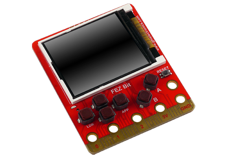
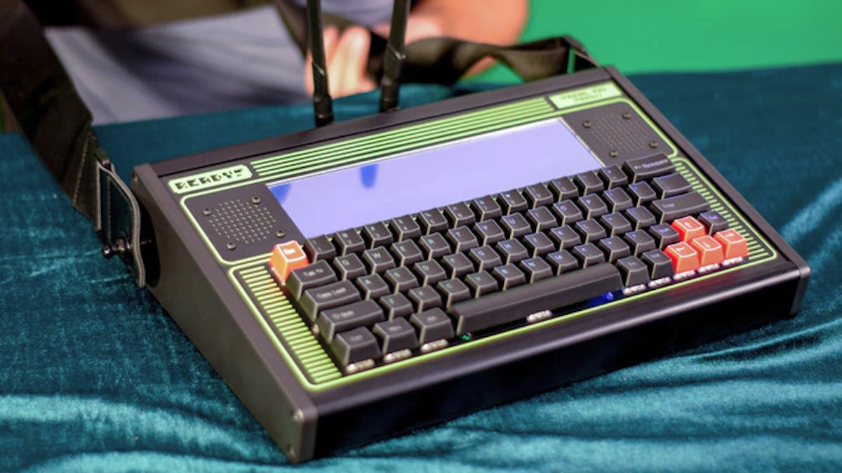
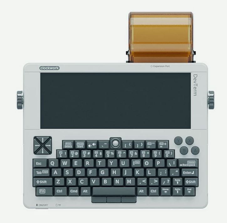
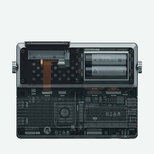
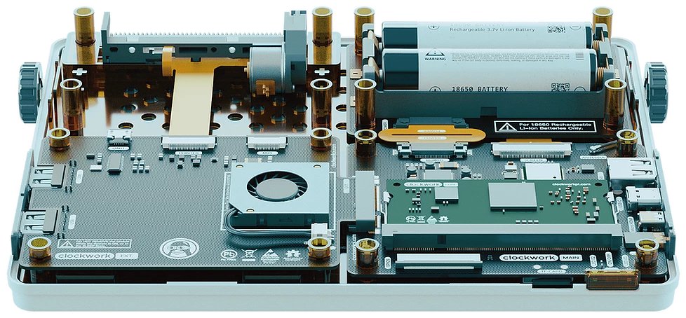

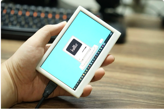
On second thought, it makes the device double the size, quite heavy and there is the problem of how to mount the screen or disconnect/re-lock it in place. Perhaps I should just get a mini battery powered hdmi screen that it can plug in to ? I could even have a cool twirly wire going to it from the device. A usb battery bank also seems like a smart way to avoid having to do all that power management and boosting with batteries on the board.
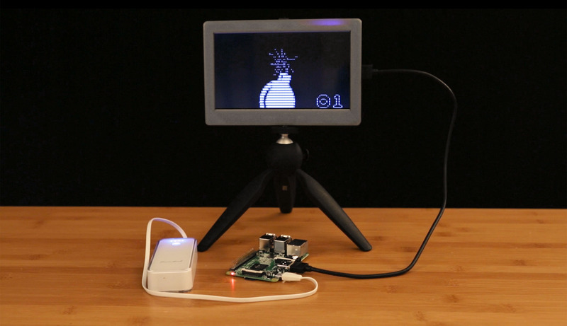
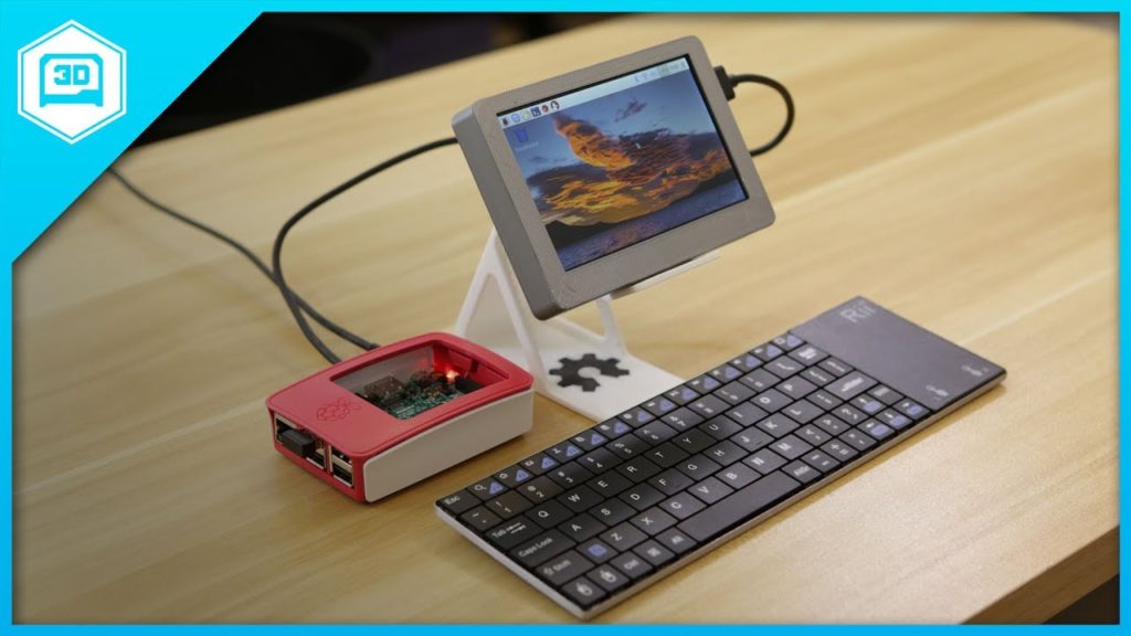
****
Took some nice photos of recent synths :
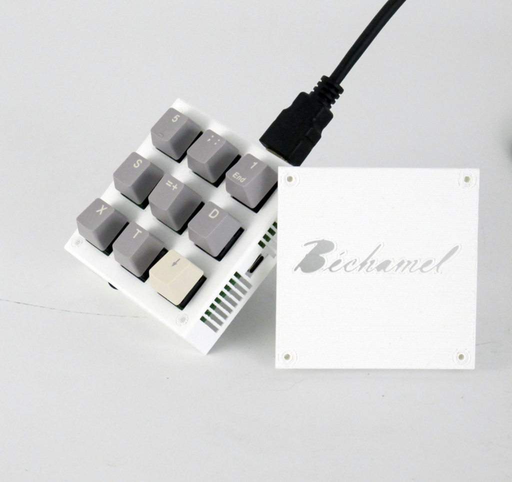
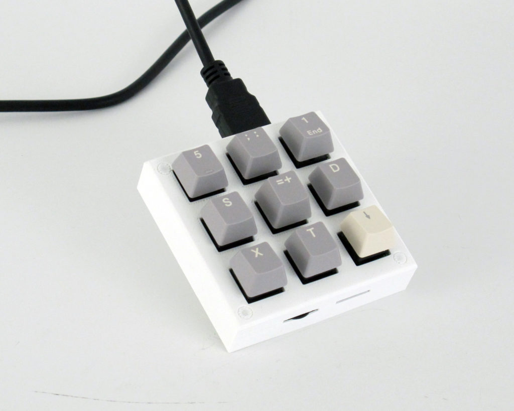
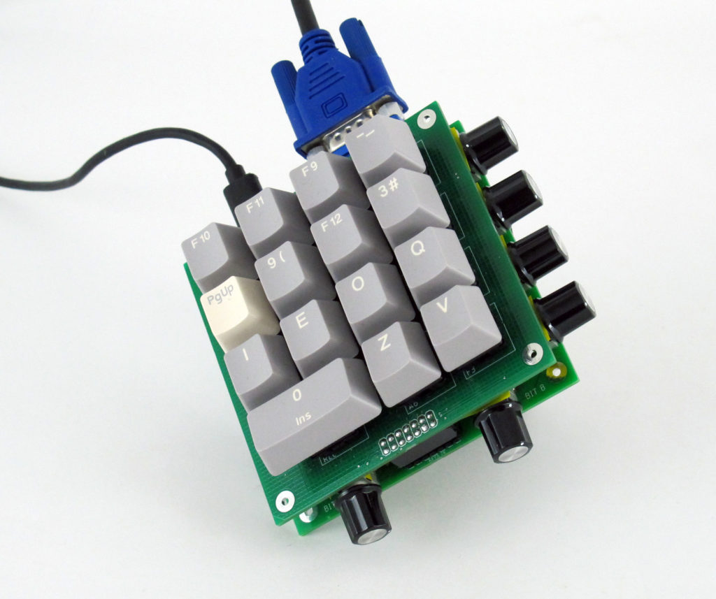
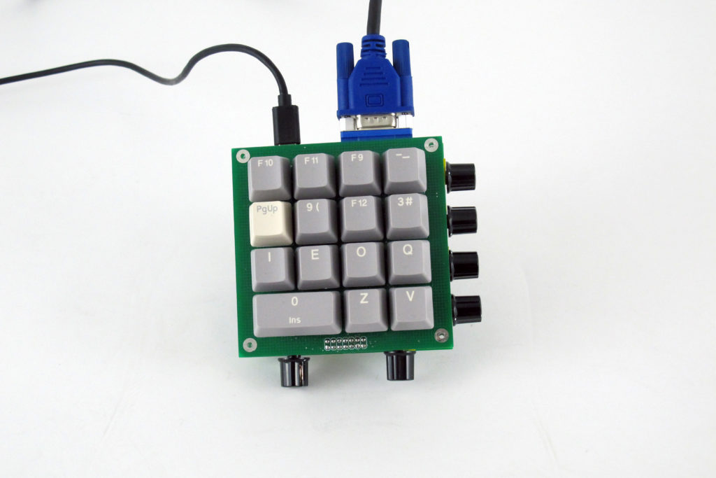
****
Finally changed Notepad++ interface to midnight and set it to interpret verilog. Fewer errors due to begin…end mismatches and mispellings. Also easier on the eyes !
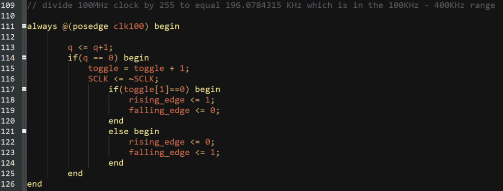
****
Tough day at the lab !
SPI has fewer steps overall, better docs but SPI requires doing thing during positive and negative edge of clock. So you need to do things every time there is a change in the state of the SCLK, so a clock that has a positive edge 2x faster than SCLK. You need two registers to tell us if we’re in rising or falling clock. (It appears that you can’t use both posedge and negedge in a single verilog even though it will work in a testbench.) This resource, and the others it links to, is still the best I can find : http://www.dejazzer.com/ee379/lecture_notes/lec12_sd_card.pdf
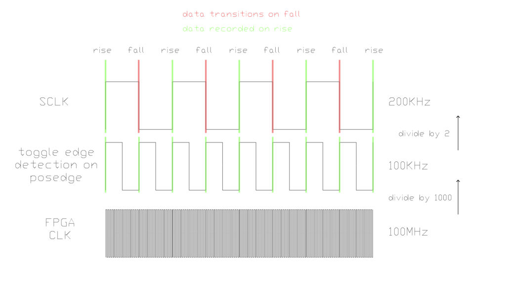
I’m working in test bench for the SPI code, and I can confirm the SCLK and toggle detection signals. For some reason I’m getting stuck with other always block and I can’t work out why at the moment. For some reason when I move counter and phase into the first block, both blocks seem to work, it feels a bit buggy.

Here is my code so far :
/*

From http://www.dejazzer.com/ee379/lecture_notes/lec12_sd_card.pdf
and http://elm-chan.org/docs/mmc/mmc_e.html
and the flow chart http://elm-chan.org/docs/mmc/m/sdinit.png

The master IC and the slave IC are tied with three signal lines:

SCLK (Serial Clock),
MISO (Master-In Slave-Out) and
MOSI (Master-Out Slave-In).

The contents of both 8-bit shift registers are exchanged with the shift clock driven by master IC. An
additional fourth signal:

SS (Slave Select),

is utilized to synchronize the start of packet or byte boundary
and to facilitate working with multiple slave devices simultaneously.

The CS signal must be driven high to low prior to send a command frame
and held it low during the transaction (command, response and data transfer if exist).


In SPI, data shift and data latch are done on opposite clock edges.

We're in Mode 0 :
Positive Pulse.
Latch, then Shift.
(CPHA=0, CPOL=0)

This means that data can only change state when the clock is transitioning from HIGH to LOW (the NEG edge).
These new values are then recorded on the positive edge.

This means that sending data (MOSI) is syncronized with the neg edge, but recording data in (MISO) is syncronized with the pos edge.

(bit 47) (bit 0)
01 + CMD number (6 bits) + Argument (32 bits) + CRC (7 bits) + 1
(MSB) (LSB)

To communicate with the SD card, your program has to place the SD card into the SPI mode. To do this, set
the MOSI and CS lines to logic value 1 and toggle SD CLK for at least 74 cycles.


*/

`timescale 1us/1ns

module top(
input wire clk100,
input wire reset,

input reg MISO,

output wire SCLK,
output reg MOSI,
output reg CS
);

//used to detect rising or falling edges
reg rising_edge = 0;
reg falling_edge = 0;

wire clk_change=0;

// counters
reg [7:0] q=0;
reg [9:0] counter=0;
reg [7:0] phase=0;
reg [9:0] wait_counter=0;

// to hold incoming message
reg [7:0] response = 0;

//CMD0 “GO_IDLE_STATE”
parameter CMD0 = 48'b01000000_00000000_00000000_00000000_00000000_10010101;

//CMD8 “SEND_IF_COND”
parameter CMD8 = 48'b01001000_00000000_00000000_00000001_10101010_10000111;

//CMD55 “APP_CMD”
parameter CMD55 = 48'b01110111_00000000_00000000_00000000_00000000_01100101;

//ACMD41 “SD_SEND_OP_COND”
parameter ACMD41 = 48'b01101001_01000000_00010000_00000000_00000000_11001101;

//CMD2 “ALL_SEND_CID”
parameter CMD2 = 48'b01000010_00000000_00000000_00000000_00000000_01001101;

//CMD3 “SEND_RELATIVE_ADDR”
parameter CMD3 = 48'b01000011_00000000_00000000_00000000_00000000_00100001;

//CMD7 “SELECT/DESELECT_CARD”
parameter CMD7 = 48'b01000111_00000000_00000001_00000000_00000000_11011101; // ASSUMING RCA IS 0001

//CMD17 “READ_SINGLE_BLOCK”
parameter CMD17 = 48'b01010001_00000000_00000000_00000000_00000000_01010101; // ASSUMING ADDR ZERO EXISTS

//CMD18 “READ_MULTIPLE_BLOCK”
parameter CMD18 = 48'b01010010_00000000_00000000_00000000_00000000_11100001; // ASSUMING ADDR ZERO EXISTS

assign SCLK = rising_edge;// toggle SCLK every 256 clock100 cycles

assign clk_change = (q[7] == 0) ? 1 : 0;
// divide 100MHz clock by 256 which is in the 100KHz - 400KHz range

always @(posedge clk100) begin

q <= q+1;

if(q[7] == 0) begin
// every 127 clock100 cycles detect which edge we're currently on
rising_edge <= 1;
falling_edge <= 0;
end
else begin
rising_edge <= 0;
falling_edge <= 1;
end
end

always @(posedge clk_change) begin // positive edge every transition of SCLK


counter <= counter+1; // WHEN I MOVE THIS TO THE FIRST BLOCK IT WORKS BUT NOT HERE FOR SOME REASON
if (counter <= 400) begin
counter<=counter;
end
else begin
counter<=0;
phase<=phase+1;
end

// Place SD in SPI Mode
if ((phase == 1) && (falling_edge==1)) begin

counter <= counter+1;

if (counter <= 75) begin
CS <= 1'b1; // DESELECT
MOSI <= 1'b1;

end
else begin
counter<=0;
phase<=phase+1;
end
end

// CMD0
if ((phase == 2) && (falling_edge==1)) begin

counter <= counter+1;
CS <= 1'b0; // SELECT

if (counter <= 47) begin
MOSI <= CMD0[counter];
end
else begin
counter<=0;
phase<=phase+1;
end
end

// Listen to MISO, we want to receive: (00000001)2
// but it takes a few clock cycles to get a message,
// so wait max 16 cycles until receive a zero on MISO
// we have to send high on MOSI during this time

if ((phase == 3) && (rising_edge==1)) begin

CS <= 1'b0; // SELECT

if (MISO == 0 || counter > 0) begin
counter <= counter+1;

if (counter <= 7) begin
response[counter] <= MISO;
MOSI<=1;
end
else begin
counter<=0;
phase<=phase+1;
end
end

else begin
//after 16 clock cycles with no response we try again
wait_counter <= wait_counter+1;

if (wait_counter >= 15) begin
CS <= 1'b1; // DESELECT
phase<=0;
end

end
end


// CMD8
if ((phase == 4) && (falling_edge==1)) begin

counter <= counter+1;
CS <= 1'b1; // DESELECT

if (response == 7'b00000001) begin

if (counter <= 47) begin
CS <= 1'b0; // SELECT
MOSI <= CMD8[counter];
end
else begin
counter<=0;
phase<=phase+1;
end
end
end

end

endmodule
****
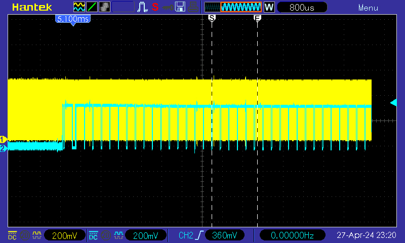
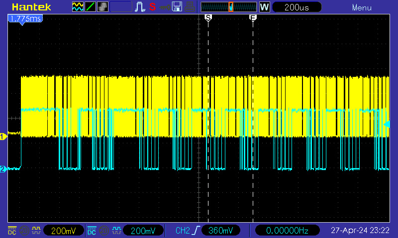
I am doing more research and also am listening to the Arduino communicate with an SD card on the ‘scope. I can’t find my logic analyzer but I have increased the memory of a trigger recording on the ‘scope so I can see a fair amount of the conversation.
We have :
- Wait
- Place SD in SPI mode
- CMD0
- CMD8
- CMD55
- ACMD41
then repeating CMD55 + ACMD41 until the end of the recording.
This image (from http://elm-chan.org/docs/mmc/mmc_e.html#spimode) helps explain my earlier mistakes :

- Preliminary stuff : The card is ready to receive a command frame when it drives DO high (from http://elm-chan.org/docs/mmc/mmc_e.html#spimode).
- The NCR is a response time which varies between 0 and 8 clock cycles, but it can take longer than this to respond! Because of this, I have to DETECT the first 0 from the SD card (WHILE of course keeping DI HIGH OxFF), then COUNT 8 bits (for an R1 response), then INTERPRET the message.
- The CS signal must be driven high to low prior to send a command frame and held it low during the transaction (command, response and data transfer if exist) (from http://elm-chan.org/docs/mmc/mmc_e.html#spimode).
From wikipedia (https://en.wikipedia.org/wiki/Serial_Peripheral_Interface) explaining the pseudo code of bit-banging SPI as master :

- Initialize SCLK as low and CS as high
- Pull CS low to select the sub
- Loop for however many number of bytes to transfer:[note 9]
- Initialize
byte_outwith the next output byte to transmit - Loop 8 times:
- Left-Shift[note 10] the next output bit from
byte_outto MOSI - NOP for the sub’s setup time
- Pull SCLK high
- Left-Shift the next input bit from MISO into
byte_in - NOP for the sub’s hold time
- Pull SCLK low
- Left-Shift[note 10] the next output bit from
byte_innow contains that recently-received byte and can be used as desired
- Initialize
- Pull CS high to unselect the sub
I think I should build a shift register, put it in a module, and use it like a function. Just did the exercise on hdlbits :
module top_module(
input clk,
input areset,
input load,
input ena,
input [3:0] data,
output reg [3:0] q);

// Asynchronous reset: Notice the sensitivity list.
// The shift register has four modes:
// reset
// load
// enable shift
// idle -- preserve q (i.e., DFFs)
always @(posedge clk, posedge areset) begin
      if (areset) // reset
          q <= 0;
      else if (load) // load
          q <= data;
      else if (ena) // shift is enabled
         q <= q[3:1]; // Use vector part select to express a shift.
end

endmodule
****
Got a logic analyzer now that decodes SPI, changes everything !
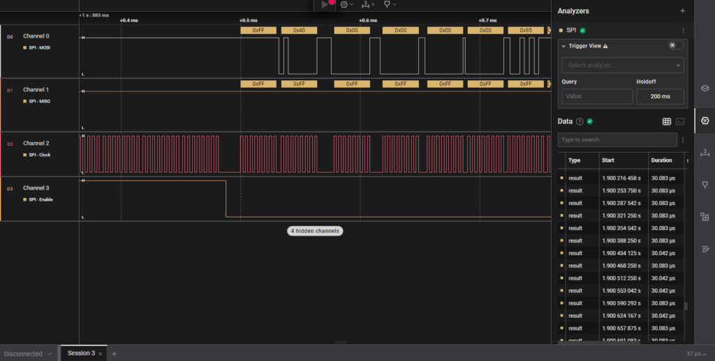
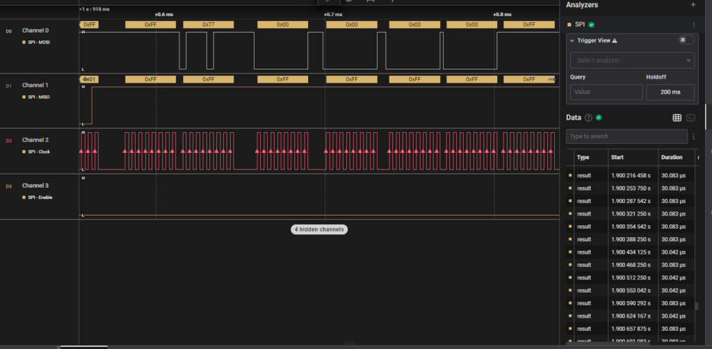
I was able to decode the conversation and it took more than 125ms for the SD to send a ready bit after the CMD55+ACMD41 requests. After the response, CMD58 was sent and with R1 response as 00 C0 FF 80 00. After this the CS was set HIGH and the clock speed was ramped way up (because it read the TRAN_SPEED field in the CSD register?). Then CMD17 for READ_SINGLE_BLOCK was sent, there was a response then a delay before some data was sent on MISO. (At this point I could send CMD18 for READ_MULTIPLE_BLOCK instead and be receiving data continuously ?)
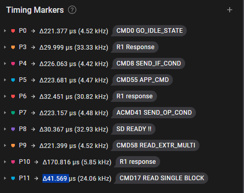
Some thoughts :
- If I were to make a product with an SD card I would need to ship it with a specific SD card type, as my code wouldn’t be flexible enough to adapt to different kinds of cards, find best speeds etc. I would need to use a proper SD card library to run on the FPGA, which would require me learning how to do that and would require some space on the FPGA and probably a larger FPGA as a result.
- It I had a microchip to handle the interaction with the SD card I think it would be a small compromise but would make life considerably easier for me.
- I had previously imagined that the majority of the data being sent from the SD card could represent images and that this could just be channeled directly to a video out. I don’t think this is very realistic, most of the data is waiting for things to be ready, sending info before and after the actual data which represents a small amount of things. Basically there is a step after which is digesting the received data and repackaging it to the FPGA I would say.
- I could prepare this step by doing some tests getting Arduino to send image data from the SD card to the FPGA to see how hard this is for me.
****
I also am taking a new approach, use the SPI_master library from NANDLAND (https://github.com/nandland/spi-master/blob/master/Verilog/source/SPI_Master.v)
I’ve started a code which compiles (!) and which references the SPI_Master.v file with this :
module top(

input wire clk100,
input wire reset,
input wire MISO,
output wire SCLK,
output wire MOSI,
output reg CS

);

reg [7:0] TX_Byte=0; // Byte to transmit on MOSI
reg TX_DV=0; // Data Valid Pulse with i_TX_Byte
wire TX_Ready=0; // Transmit Ready for next byte
wire RX_DV=0; // Data Valid pulse (1 clock cycle)
wire [7:0] RX_Byte=0; // Byte received on MISO

....

SPI_Master (

.i_Rst_L(reset),
.i_Clk(clk100),
.i_TX_Byte(TX_Byte), // Byte to transmit on MOSI
.i_TX_DV(TX_DV), // Data Valid Pulse with i_TX_Byte
.o_TX_Ready(TX_Ready), // Transmit Ready for next byte
.o_RX_DV(RX_DV), // Data Valid pulse (1 clock cycle)
.o_RX_Byte(RX_Byte), // Byte received on MISO
.o_SPI_Clk(SCLK),
.i_SPI_MISO(MISO),
.o_SPI_MOSI(MOSI)

);

endmodule //module top
I can’t figure out how to make a testbench with it yet.
CMD0 arg: 0x0, CRC: 0x95 (response: 0x01) – note that in case of 0xFF or garbled response you should simply repeat this step; see below for more info.
CMD8 arg: 0x000001AA, CRC: 0x87 (response: 0x01, followed by echo of arg, in this case 0x000001AA) – while it may seem that this command is optional, it’s completely mandatory for newer cards. While 0x1AA is a common arg value here, you may actually pass other values as well; see “Table 7-5: Card Operation for CMD8 in SPI Mode”, p. 108 in spec for details.
3a. CMD55 arg: 0x0, CRC: any, 0x65 actually (response: 0x01; CMD55 being the prefix to every ACMD; if the response is 0x05, you’ve got an old card – repeat CMD1 with arg 0x0 [CRC 0xF9] instead of CMD55/ACMD41)
3b. ACMD41 , arg: 0x40000000, CRC: any, 0x77 actually (note that this argument assumes the card is a HCS one, which is usually the case; use 0x0 arg [CRC 0xE5] for older cards). If response is 0x0, you’re OK; if it’s 0x01, goto 3a; if it’s 0x05, see note on it above (in 3a.); if it’s neither, something’s wrong with it (also see below).
****
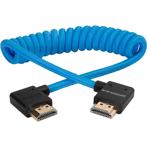
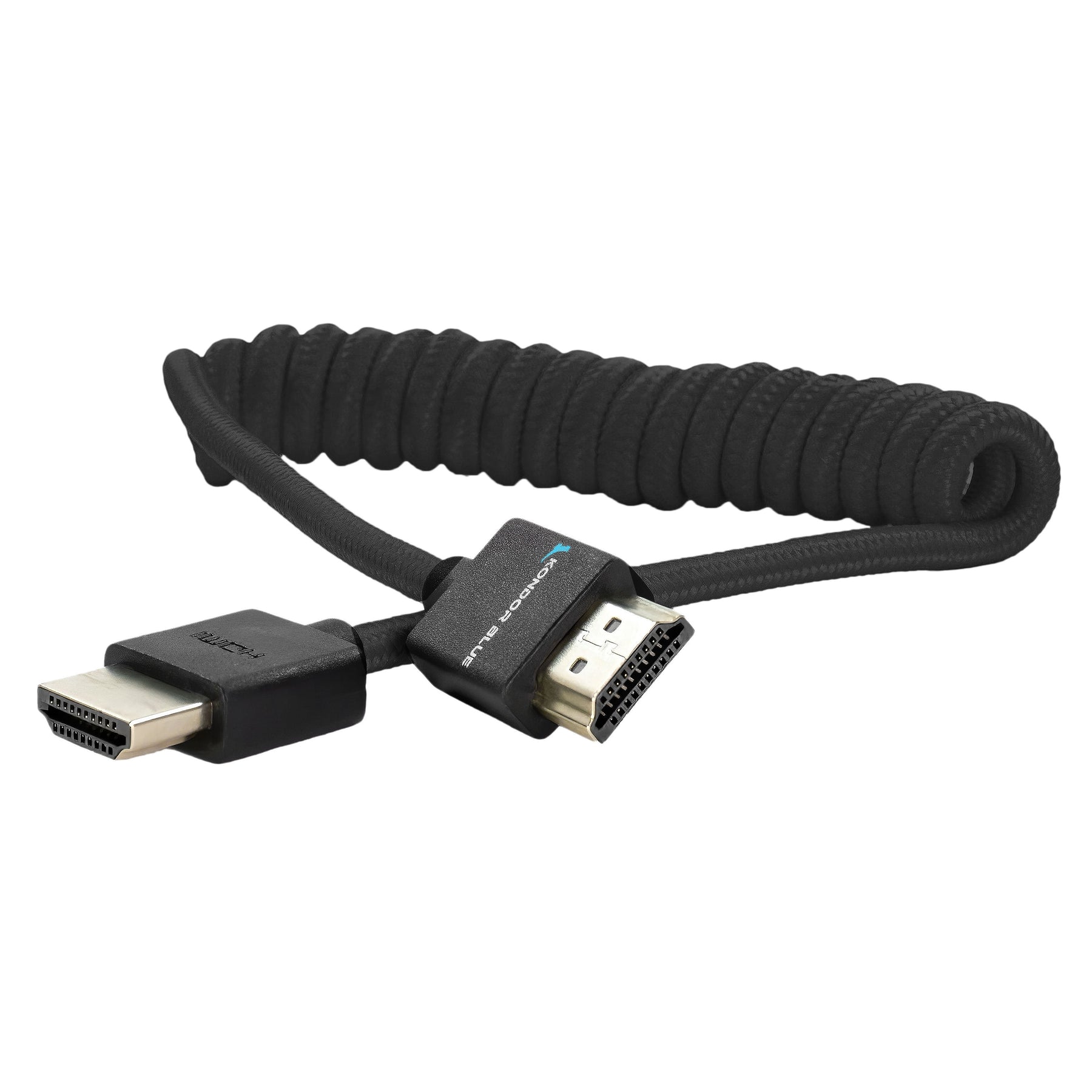
`default_nettype none // disable implicit definitions by Verilog
//-----------------------------------------------------------------
// minimalDVID_encoder.vhd : A quick and dirty DVI-D implementation
//
// Author: Mike Field <hamster@snap.net.nz>
//
// DVI-D uses TMDS as the 'on the wire' protocol, where each 8-bit
// value is mapped to one or two 10-bit symbols, depending on how
// many 1s or 0s have been sent. This makes it a DC balanced protocol,
// as a correctly implemented stream will have (almost) an equal
// number of 1s and 0s.
//
// Because of this implementation quite complex. By restricting the
// symbols to a subset of eight symbols, all of which having have
// five ones (and therefore five zeros) this complexity drops away
// leaving a simple implementation. Combined with a DDR register to
// send the symbols the complexity is kept very low.
//-----------------------------------------------------------------

module top(
clk100, key, hdmi_p, hdmi_n, reset
);

input reset;
input clk100;
input [8:0] key;
output [3:0] hdmi_p;
output [3:0] hdmi_n;

// to store values from other modules
wire half_sec;

wire [12:0] random_number_0;
wire [12:0] random_number_1;
wire [12:0] random_number_2;
wire [12:0] random_number_3;
wire [12:0] random_number_4;
wire [12:0] random_number_5;
wire [12:0] random_number_6;
wire [12:0] random_number_7;
wire [12:0] random_number_8;
wire [12:0] random_number_9;
wire [7:0] sine_wave;

// for our bittiness
wire [9:0] bit_or;
assign bit_or = hc[9:0]|vc[9:0];

wire [9:0] bit_xor;
assign bit_xor = hc[9:0]^vc[9:0];

wire [9:0] bit_and;
assign bit_and = hc[9:0]&vc[9:0];

wire [9:0] bit_nand;
assign bit_nand = hc[9:0]& ~vc[9:0];

wire [9:0] bit_xnor;
assign bit_xnor = hc[9:0]^ ~vc[9:0];

reg [9:0] out_bit ;


// For holding the outward bound TMDS symbols in the slow and fast domain
reg [9:0] c0_symbol; reg [9:0] c0_high_speed;
reg [9:0] c1_symbol; reg [9:0] c1_high_speed;
reg [9:0] c2_symbol; reg [9:0] c2_high_speed;
reg [9:0] clk_high_speed;

reg [1:0] c2_output_bits;
reg [1:0] c1_output_bits;
reg [1:0] c0_output_bits;
reg [1:0] clk_output_bits;

wire clk_x5;
reg [2:0] latch_high_speed = 3'b100; // Controlling the transfers into the high speed domain

wire vsync, hsync;
wire [1:0] syncs; // To glue the HSYNC and VSYNC into the control character
assign syncs = {vsync, hsync};

// video structure constants
parameter hpixels = 800; // horizontal pixels per line
parameter vlines = 525; // vertical lines per frame
parameter hpulse = 96; // hsync pulse length
parameter vpulse = 2; // vsync pulse length
parameter hbp = 144; // end of horizontal back porch (96 + 48)
parameter hfp = 784; // beginning of horizontal front porch (800 - 16)
parameter vbp = 35; // end of vertical back porch (2 + 33)
parameter vfp = 515; // beginning of vertical front porch (525 - 10)

// registers for storing the horizontal & vertical counters
reg [9:0] vc;
reg [9:0] hc;
// generate sync pulses (active high)
assign vsync = (vc < vpulse);
assign hsync = (hc < hpulse);

always @(posedge clk_x5) begin
//-------------------------------------------------------------
// Now take the 10-bit words and take it into the high-speed
// clock domain once every five cycles.
//
// Then send out two bits every clock cycle using DDR output
// registers.
//-------------------------------------------------------------
c0_output_bits <= c0_high_speed[1:0];
c1_output_bits <= c1_high_speed[1:0];
c2_output_bits <= c2_high_speed[1:0];
clk_output_bits <= clk_high_speed[1:0];
if (latch_high_speed[2]) begin // pixel clock 25MHz
c0_high_speed <= c0_symbol;
c1_high_speed <= c1_symbol;
c2_high_speed <= c2_symbol;
clk_high_speed <= 10'b0000011111;
latch_high_speed <= 3'b000;
if (hc < hpixels)
hc <= hc + 1;
else
begin
hc <= 0;
if (vc < vlines)
vc <= vc + 1;
else
vc <= 0;
end
end
else begin
c0_high_speed <= {2'b00, c0_high_speed[9:2]};
c1_high_speed <= {2'b00, c1_high_speed[9:2]};
c2_high_speed <= {2'b00, c2_high_speed[9:2]};
clk_high_speed <= {2'b00, clk_high_speed[9:2]};
latch_high_speed <= latch_high_speed + 1'b1;
end
end

always @(*) // display 100% saturation colourbars
begin
// first check if we're within vertical active video range
if (vc >= vbp && vc < vfp)
begin
// now display different colours every 80 pixels
// while we're within the active horizontal range
// -----------------
// display white bar

if (hc >= hbp && hc < hfp && (bit_xor[8:0] == key[8:0]))
begin
c2_symbol = 10'b1011110000; // red
c1_symbol = 10'b1011110000; // green
c0_symbol = 10'b1011110000; // blue
end
// display black bar
else if (hc >= hbp && hc < hfp)
begin
c2_symbol = 10'b0111110000; // red
c1_symbol = 10'b0111110000; // green
c0_symbol = 10'b0111110000; // blue
end
// we're outside active horizontal range
else
begin
c2_symbol = 10'b1101010100; // red
c1_symbol = 10'b1101010100; // green
//---------------------------------------------
// Channel 0 carries the blue pixels, and also
// includes the HSYNC and VSYNCs during
// the CTL (blanking) periods.
//---------------------------------------------
case (syncs)
2'b00 : c0_symbol = 10'b1101010100;
2'b01 : c0_symbol = 10'b0010101011;
2'b10 : c0_symbol = 10'b0101010100;
default : c0_symbol = 10'b1010101011;
endcase
end
end
// we're outside active vertical range
else
begin
c2_symbol = 10'b1101010100; // red
c1_symbol = 10'b1101010100; // green
//---------------------------------------------
// Channel 0 carries the blue pixels, and also
// includes the HSYNC and VSYNCs during
// the CTL (blanking) periods.
//---------------------------------------------
case (syncs)
2'b00 : c0_symbol = 10'b1101010100;
2'b01 : c0_symbol = 10'b0010101011;
2'b10 : c0_symbol = 10'b0101010100;
default : c0_symbol = 10'b1010101011;
endcase
end
end

// red N
defparam hdmin2.PIN_TYPE = 6'b010000;
defparam hdmin2.IO_STANDARD = "SB_LVCMOS";
SB_IO hdmin2 (
.PACKAGE_PIN (hdmi_n[2]),
.CLOCK_ENABLE (1'b1),
.OUTPUT_CLK (clk_x5),
.OUTPUT_ENABLE (1'b1),
.D_OUT_0 (~c2_output_bits[1]),
.D_OUT_1 (~c2_output_bits[0])
);

// red P
defparam hdmip2.PIN_TYPE = 6'b010000;
defparam hdmip2.IO_STANDARD = "SB_LVCMOS";
SB_IO hdmip2 (
.PACKAGE_PIN (hdmi_p[2]),
.CLOCK_ENABLE (1'b1),
.OUTPUT_CLK (clk_x5),
.OUTPUT_ENABLE (1'b1),
.D_OUT_0 (c2_output_bits[1]),
.D_OUT_1 (c2_output_bits[0])
);

// green N
defparam hdmin1.PIN_TYPE = 6'b010000;
defparam hdmin1.IO_STANDARD = "SB_LVCMOS";
SB_IO hdmin1 (
.PACKAGE_PIN (hdmi_n[1]),
.CLOCK_ENABLE (1'b1),
.OUTPUT_CLK (clk_x5),
.OUTPUT_ENABLE (1'b1),
.D_OUT_0 (~c1_output_bits[1]),
.D_OUT_1 (~c1_output_bits[0])
);

// green P
defparam hdmip1.PIN_TYPE = 6'b010000;
defparam hdmip1.IO_STANDARD = "SB_LVCMOS";
SB_IO hdmip1 (
.PACKAGE_PIN (hdmi_p[1]),
.CLOCK_ENABLE (1'b1),
.OUTPUT_CLK (clk_x5),
.OUTPUT_ENABLE (1'b1),
.D_OUT_0 (c1_output_bits[1]),
.D_OUT_1 (c1_output_bits[0])
);


// blue N
defparam hdmin0.PIN_TYPE = 6'b010000;
defparam hdmin0.IO_STANDARD = "SB_LVCMOS";
SB_IO hdmin0 (
.PACKAGE_PIN (hdmi_n[0]),
.CLOCK_ENABLE (1'b1),
.OUTPUT_CLK (clk_x5),
.OUTPUT_ENABLE (1'b1),
.D_OUT_0 (~c0_output_bits[1]),
.D_OUT_1 (~c0_output_bits[0])
);

// blue P
defparam hdmip0.PIN_TYPE = 6'b010000;
defparam hdmip0.IO_STANDARD = "SB_LVCMOS";
SB_IO hdmip0 (
.PACKAGE_PIN (hdmi_p[0]),
.CLOCK_ENABLE (1'b1),
.OUTPUT_CLK (clk_x5),
.OUTPUT_ENABLE (1'b1),
.D_OUT_0 (c0_output_bits[1]),
.D_OUT_1 (c0_output_bits[0])
);

// clock N
defparam hdmin3.PIN_TYPE = 6'b010000;
defparam hdmin3.IO_STANDARD = "SB_LVCMOS";
SB_IO hdmin3 (
.PACKAGE_PIN (hdmi_n[3]),
.CLOCK_ENABLE (1'b1),
.OUTPUT_CLK (clk_x5),
.OUTPUT_ENABLE (1'b1),
.D_OUT_0 (~clk_output_bits[1]),
.D_OUT_1 (~clk_output_bits[0])
);


// clock P
defparam hdmip3.PIN_TYPE = 6'b010000;
defparam hdmip3.IO_STANDARD = "SB_LVCMOS";
SB_IO hdmip3 (
.PACKAGE_PIN (hdmi_p[3]),
.CLOCK_ENABLE (1'b1),
.OUTPUT_CLK (clk_x5),
.OUTPUT_ENABLE (1'b1),
.D_OUT_0 (clk_output_bits[1]),
.D_OUT_1 (clk_output_bits[0])
);
// D_OUT_0 and D_OUT_1 swapped?
// https://github.com/YosysHQ/yosys/issues/330


SB_PLL40_PAD #(
.FEEDBACK_PATH ("SIMPLE"),
.DIVR (4'b0000),
.DIVF (7'b0001001),
.DIVQ (3'b011),
.FILTER_RANGE (3'b101)
) uut (
.RESETB (1'b1),
.BYPASS (1'b0),
.PACKAGEPIN (clk100),
.PLLOUTGLOBAL (clk_x5) // DVI clock 125MHz
);

LFSR random_s(
.clock(clk100),
.reset(reset),
.half_sec_pulse(half_sec),
.rnd_0(random_number_0),
.rnd_1(random_number_1),
.rnd_2(random_number_2),
.rnd_3(random_number_3),
.rnd_4(random_number_4),
.rnd_5(random_number_5),
.rnd_6(random_number_6),
.rnd_7(random_number_7),
.rnd_8(random_number_8),
.rnd_9(random_number_9)
);

sine_wave_gen sine_wave_s(
.clk(clk100),
.data_out(sine_wave)
);

tempo tempo_s(
.clk(clk100),
.half_sec_pulse(half_sec)
);


endmodule
*****
Nothing is easy today. Put the FPGA in pass-though mode taking rpi color info in and outputing HDMI and nothing seems to be working.
- the rpi on the CC board should be powered by 5V and not 3.3V.
- I put the mirror of the typical rpi header situation on the board, which requires the header to be put under the board…
- the rpi seems to pull too much power to be plugged in to the FPGA board. I should see if this is still the case after powering directly from the 5V from USB instead of the 5V post PFET.
- Perhaps 125MHz is so fast that sampling the slower incoming video from the rpi was never going to work without using the H and V sync. I was expecting a badly distorted image but what I’m seeing is just thick white bands. Next step would be to take in rpi H, V and pixel clock, and to use these to display images.
*EDIT* I’ve confirmed that the rpi is super power hungry and cannot be powered by the same power supply as the FPGA, even if connected before the fuse. What works currently is me plugging it in seperately and then just jumping the necessary wires to the board.
****
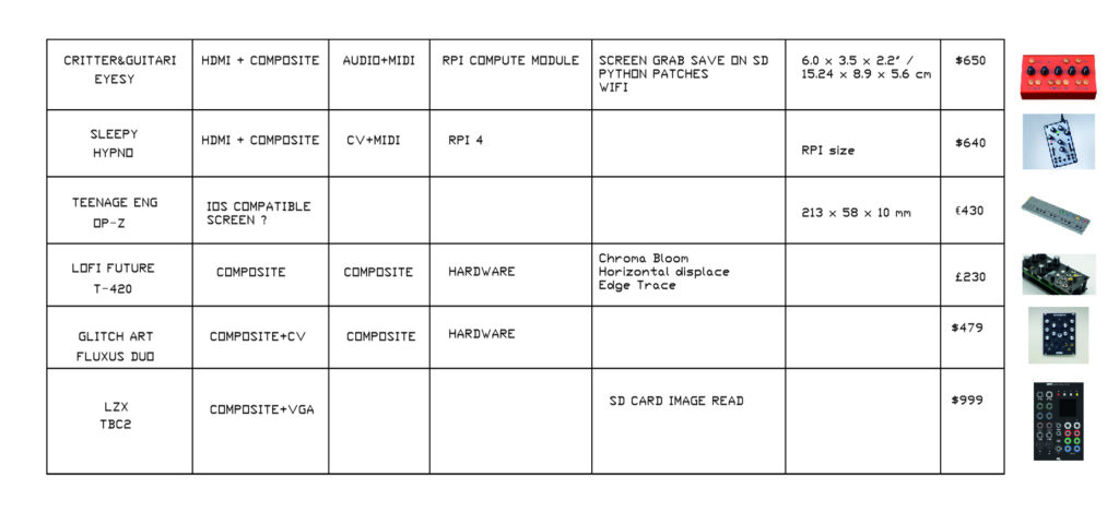
For these (https://www.reddit.com/r/synthesizers/comments/1626o2k/recommend_some_hardware_video_synthesizers/?share_id=4daCLEXF208G0iw0aUnJD&utm_content=1&utm_medium=android_app&utm_name=androidcss&utm_source=share&utm_term=1) and other video synth boards I want to make a table with price, video in, video out, etc.
Just starting this and I’m realizing that there are some €400-600 expensive video synths that are just rpis (called compute modules which don’t have any conectors) with knobs. The analog video synths seem to be more composite video focused and eurorack compatible. People are selling these on etsy. There is also the refurbished, spray painted, and circuit bent video devices, digital cameras, from the 90s + 2000s market.
This brand has nice design : https://www.afterlifelaboratories.com/
The 100×100 pixel bitmaps I output with ffmpeg are 10.8KB each. If I had three frames a second, I could store an hour of film in
Also watch spi tutorial and debug with the Arduino sd card !! Will then have proved my understanding and will have oscilloscope/ Logic analyser recordings
****
After the experience trying to create an SD interface in verilog, and some reflection on the complexity of reconstructing high speed HDMI video from SD bmp stills incoming at a completely different speed, I’ve been reconsidering the TFP401A Digital Receiver chip (7 euros). It would essentially be like the rpi in DPI mode (it outputs DE, HSYNC, VSYNC, Pixel CLK, etc.) but much faster and with some configuration options to play with (staggering off/on, odd or even color sel, one/two pixels per clock sel, output drive strength sel).
Instead of generating signals with the FPGA, could I also take timing signals from the chip ?
This approach seems to be the most pragmatic for a viable video synth product. After it would be just having fun coding with video in and out.
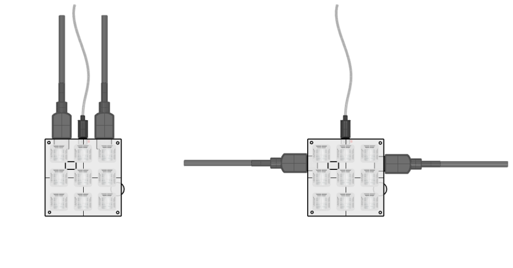
Two possibilities for double HDMI plugs. Left is way more convenient.
****
Sam’s advice :
- Think about language around the product, naming aspects. “Rewilding circuits !” “Post-colonial circuitry”
- More deliberate about the screen selection, bigger screen or screen selected for the experience of watching ?
- Culture of where buttons are in synth culture, play them to learn.
- Ergonomics ?!
Check out funky Rule90 esque thing :

*****
Trying to get potentiometer reading working based on this post https://web.archive.org/web/20191115162412/http://hamsterworks.co.nz/mediawiki/index.php/Cheap_Analogue_Input :
reg [18:0] adc_count= 0; //to count how long it's taking to charge
reg [16:0] pot_value= 0; //to store cap charge time value

reg [12:0] counter = 0;

wire adc_in = 0;
reg adc_sample = 0;

assign adc = (adc_sample) ? 1'bZ : 1'b0;
assign adc_in = adc;

always @(posedge latch_high_speed[2]) begin
counter = counter + 1;
                if (counter==0) begin

                               adc_count <= adc_count + 1; // start counting

                                               if(adc_count==0)begin // once we have rolled over counter...

                                                               adc_sample <= 1'b0; // discharge cap to restart the process

                                               end

                                               if(adc_count==19'b1111111111111111111)begin // if max amount of time has passed
                                                               pot_value <=17'b11111111111111111; //store max value in pot

                                               end

                                               else begin

                                                               if(adc_in==1) begin // if cap charged...

                                                                               pot_value<=adc_count[18:2]; // top 17 bits are pot

                                                               end

                                                      adc_sample<=1'b1; //put cap pin in high 'Z'

                                               end
                end
end
Later on I check to see the value of pot_value in order to draw pixels or not :
if (hc >= hbp && hc < hfp && (out_bit[8:0] == key[8:0]) && (pot_value < 17'b11111000000000000))begin
...
end
FAST CHARGE :

Fastest charging time possible is when the 10K is set at zero. The resistance in that case is just the 1K resistor in series.
The time it takes the cap to charge in this case is is 0.7 x tau = 0.00007 seconds.
I’m using 25MHz clock which takes 1,750 cycles (with a period of 0.00000004 seconds) to count that long.
SLOW CHARGE :
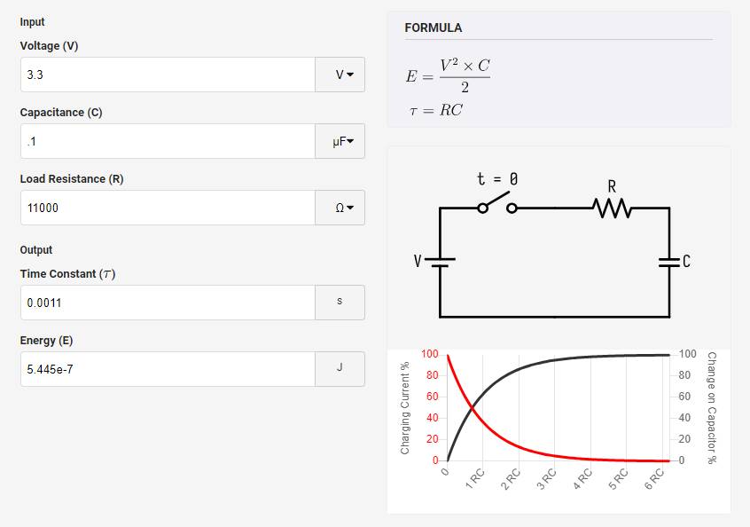
Slowest charging time possible is when the 10K is set at full. The resistance in that case is 10K + the 1K resistor in series.
The time it takes the cap to charge in this case is is 0.7 x tau = 0.00077 seconds.
I’m using 25MHz clock which takes 19,250 cycles (with a period of 0.00000004 seconds) to count that long.
This means I have a range of time to count between 1,750 and 19,250 cycles.
I need at least a 15 bit counter (2^15 max value of 32,768) to be able to count up to 19,250.
10,500 cycles would make a good threshold as it is between the min and the max. This is equal to 010100100000100 in binary.
****
It works ! Here is the final pot reading part of the code :
reg [15:0] adc_count= 0; //15 bits to count how long it's taking to charge. 32,768 is the max value. The MSB is to discharge the cap.
reg [14:0] pot_value= 0; //to store cap charge time value

wire adc_in;
reg adc_sample = 1; //first time through we want to sample the cap value


assign adc = (adc_sample) ? 1'bZ : 1'b0;
assign adc_in = adc;

always @(posedge latch_high_speed[2]) begin //25MHz clock

adc_count <= adc_count + 1; // start counting

if(adc_count>=16'b1000000000000000)begin // once we have rolled over 15 bit counter...

adc_sample <= 1'b0; // ...discharge cap for a while to restart the process.
end

else begin

adc_sample<=1'b1; //put cap pin in high 'Z'

if(adc_in==1'b1) begin // if cap charged...

pot_value[14:0]<=adc_count[14:0]; //store this value in pot

end


end

end
It’s a bit jumpy to look at the lower bits but taking the top 2 bits you can have a realiable dividing of the pot’s range into 4.
Looks like you can average binary numbers by just adding then and then shifting the bits to the right !
****
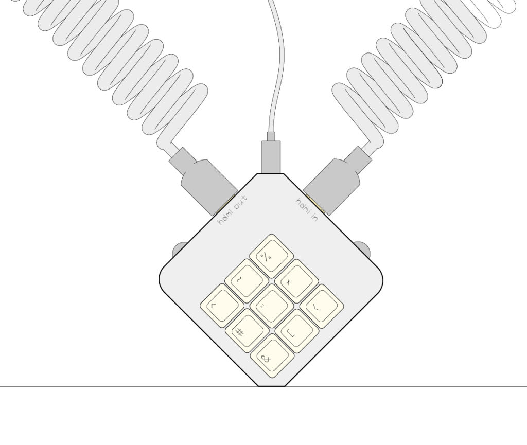
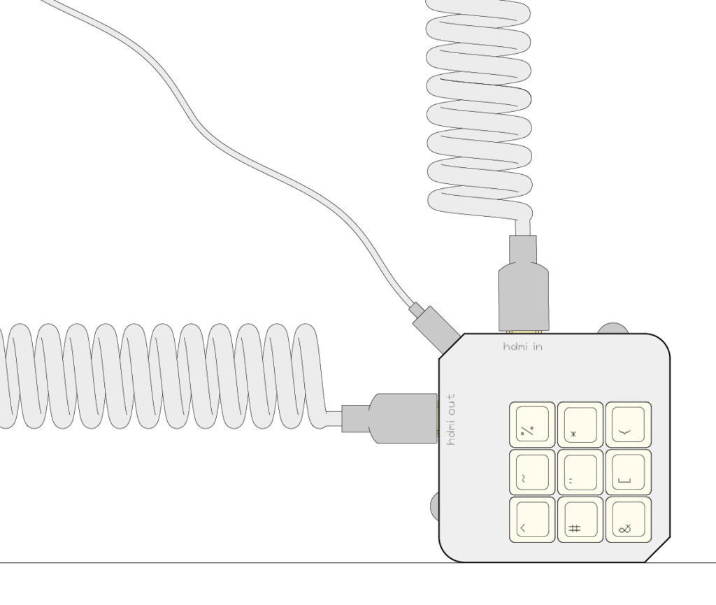
HDMI IN and OUT board with tightly packed buttons and two pots. Had some fun with chamfer vs fillet and square vs. diamond :
****
Fabien reminded me about the MILKY MIST FPGA video synth he mentioned earlier (https://m-labs.hk/gateware/m1/)
Notes from meeting with Rémi GEORGES who kindly shared many references with me :
Isohélie (https://reverb.com/fr/item/70201236-syntonie-isohelie-3-channel-3-bit-dac-keyer-for-eurorack-video-synthesis)
Eric Schlappi
Faust DST (https://faust.grame.fr/)
Grame Lyon Fast (https://fast.grame.fr/)
BPMC HDK-1 FPGA glitch (https://bpmcglitch.com/product/hdk-01/)
L’ERG école recherche graphique (https://wiki.erg.be/m/#%C3%89cole_de_recherche_graphique)
Karlsruhe live coding masters (https://hfm-karlsruhe.de/en/university/institutes/institute-music-informatics-and-musicology/courses-imwi)
Hacklabio.org zagreb fubar (https://fubar.space/)
Fflive (https://ffglitch.org/gallery/)
Vector live
A discord called Syntonie (
Recur boy – an rpi based video synth (https://github.com/cyberboy666/recurBOY)
Lintz conf
P5live (https://teddavis.org/p5live/)
Chair de poule cookie coolllectif (https://www.instagram.com/cookiecollectif/)
Raphaël Bastide (https://raphaelbastide.com/)
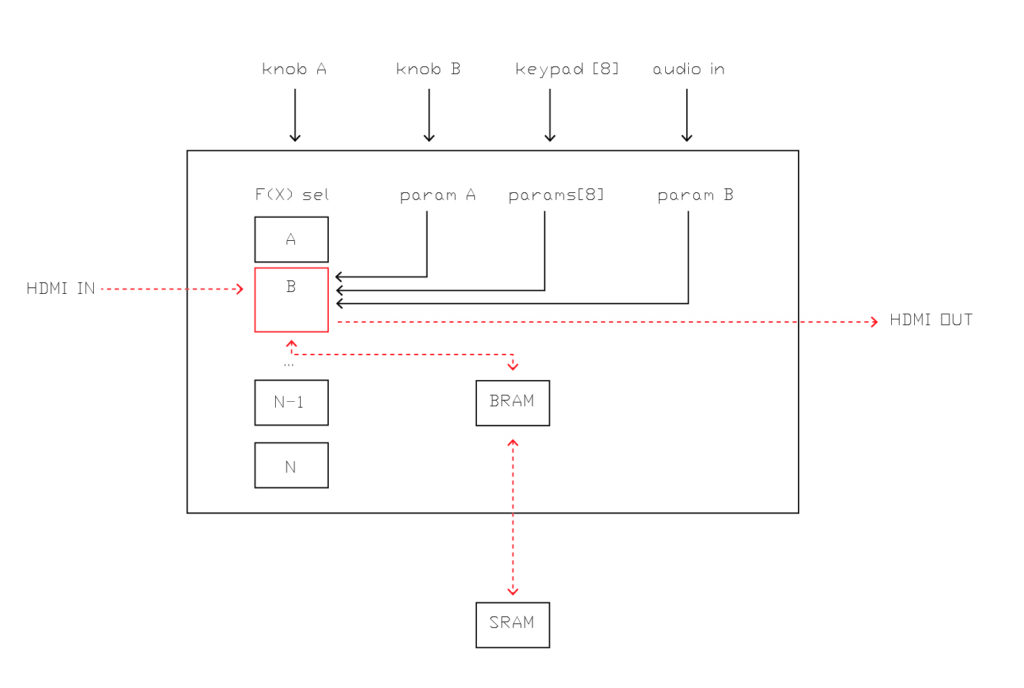
Instead of looking under every single rock on the beach I’m thinking I should only do things with this board that are not possible with Processessing on a computer. So, things that have to do with time like that heat camera and extra heavy parallel stuff ? Otherwise I am just putting myself through suffering for no real benefit as far as I can see.
****
Taking another crack at getting rpi to pass video into the Cyber Campus version of the board.
Because I didn’t include the pixel clock or DEN, I’ve made life a little harder for myself. I’ve adapted the HDMI code to change symbols based on the rpi h and v syncs.
always @(posedge rpi_pixel_clock) // display 100% saturation colourbars

begin

                // first check if we're within vertical active video range

                if (rpi_vsync)

                begin

                // now display different colours every 80 pixels
                // while we're within the active horizontal range

                // -----------------

                               if (rpi_hsync)
                               begin

                                               if ((b_in == 1'b1))
                                               begin

                                                    c2_symbol = 10'b0111110000; // red
                                                    c1_symbol = 10'b1011110000; // green
                                                    c0_symbol = 10'b1011110000; // blue

                                               end

                                               if ((b_in == 1'b0))
                                               begin

                                                    c2_symbol = 10'b1011110000; // red
                                                    c1_symbol = 10'b0111110000; // green
                                                    c0_symbol = 10'b1011110000; // blue

                                               end

                               end

                               // we're outside active horizontal range

                               else
                               begin

                                               c2_symbol = 10'b1101010100; // red
                                               c1_symbol = 10'b1101010100; // green

//---------------------------------------------

// Channel 0 carries the blue pixels, and also
// includes the HSYNC and VSYNCs during
// the CTL (blanking) periods.

//---------------------------------------------

                                               case (syncs)

                                               2'b00 : c0_symbol = 10'b1101010100;
                                               2'b01 : c0_symbol = 10'b0010101011;
                                               2'b10 : c0_symbol = 10'b0101010100;
                                               default : c0_symbol = 10'b1010101011;

                                               endcase

                               end
                end

// we're outside active vertical range

                else
                begin

                               c2_symbol = 10'b1101010100; // red
                               c1_symbol = 10'b1101010100; // green

//---------------------------------------------

// Channel 0 carries the blue pixels, and also
// includes the HSYNC and VSYNCs during
// the CTL (blanking) periods.

//---------------------------------------------

                               case (syncs)

                               2'b00 : c0_symbol = 10'b1101010100;
                               2'b01 : c0_symbol = 10'b0010101011;
                               2'b10 : c0_symbol = 10'b0101010100;
                               default : c0_symbol = 10'b1010101011;

                               endcase
                end
end
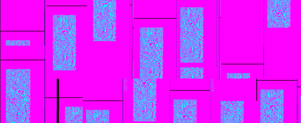
It draws the video to the left side and then has a bunch of blank space.
By changing the rpi_pixel_clock to a division of the that clock, we get multiple pi images on screen :
******
I can now record from the FPGA (not yet RPI) on the little SRAM. I had run into a few issues :
- The reset pin I selected isn’t valid according to IceCube so the always block that tested the pin didn’t work and the address didn’t count up.
- I was using one of the keys, key[8] as a reset, and the compiler didn’t like that. So I just defined in the pcf that there were only 8 keys and the 9th was not part of the array and was called rec.
On the left is the original pattern from the FPGA, on the right what the SRAM is playing back :


Here is the pcf :
set_io hdmi_p[0] 139 -io_std SB_LVCMOS
set_io hdmi_p[2] 78 -io_std SB_LVCMOS
set_io hdmi_p[1] 80 -io_std SB_LVCMOS
set_io hdmi_p[3] 137 -io_std SB_LVCMOS

set_io hdmi_n[0] 138 -io_std SB_LVCMOS
set_io hdmi_n[2] 79 -io_std SB_LVCMOS
set_io hdmi_n[1] 81 -io_std SB_LVCMOS
set_io hdmi_n[3] 136 -io_std SB_LVCMOS

set_io key[0] 37
set_io key[1] 38
set_io key[2] 39
set_io key[3] 41
set_io key[4] 42
set_io key[5] 43
set_io key[6] 44
set_io key[7] 45
set_io rec 47

set_io SCK 32
set_io CMD 33

set_io LED1 29
set_io LED5 28

set_io reset 66

set_io clk100 49

set_io b_in 63

set_io rpi_pixel_clock 61
set_io rpi_hsync 52
set_io rpi_vsync 58
set_io rpi_DEN 62

set_io v_sync 97 //for vga
set_io h_sync 76 //for vga

set_io io[0] 7
set_io io[1] 8
set_io io[2] 9
set_io io[3] 10
set_io io[4] 11
set_io io[5] 12
set_io io[6] 19
set_io io[7] 22

set_io addr[0] 4
set_io addr[1] 3
set_io addr[2] 2
set_io addr[3] 1
set_io addr[4] 144
set_io addr[5] 143
set_io addr[6] 142
set_io addr[7] 141
set_io addr[8] 120
set_io addr[9] 121
set_io addr[10] 24
set_io addr[11] 122
set_io addr[12] 135
set_io addr[13] 119
set_io addr[14] 134
set_io addr[15] 116
set_io addr[16] 129
set_io addr[17] 128


set_io cs 25
set_io oe 23
set_io we 118
Here is the verilog :
`default_nettype none // disable implicit definitions by Verilog
//-----------------------------------------------------------------
// minimalDVID_encoder.vhd : A quick and dirty DVI-D implementation
//
// Author: Mike Field <hamster@snap.net.nz>
//
// DVI-D uses TMDS as the 'on the wire' protocol, where each 8-bit
// value is mapped to one or two 10-bit symbols, depending on how
// many 1s or 0s have been sent. This makes it a DC balanced protocol,
// as a correctly implemented stream will have (almost) an equal
// number of 1s and 0s.
//
// Because of this implementation quite complex. By restricting the
// symbols to a subset of eight symbols, all of which having have
// five ones (and therefore five zeros) this complexity drops away
// leaving a simple implementation. Combined with a DDR register to
// send the symbols the complexity is kept very low.
//-----------------------------------------------------------------

module top(
clk100, hdmi_p, hdmi_n, rec, addr, io, cs, we, oe, key, reset
);


input wire rec, // the record button IS ACTIVE LOW !!
input clk100;
output [3:0] hdmi_p;
output [3:0] hdmi_n;

input reset; // 66 is not an accepted pin, DO NOT USE in ALWAYS BLOCK !

input [7:0] key;

output reg [17:0] addr;
inout wire [7:0] io; // inout must be type wire

output wire cs;
output reg we;
output wire oe;

wire [7:0] data_in;
wire [7:0] data_out;

reg [7:0] a, b;

assign io = (rec==0) ? a : 8'bzzzzzzzz; // rec==0 is when rec button pushed

assign data_out = b;

// for our bittiness
reg [9:0] again_xnor;

// registers for storing the horizontal & vertical counters
reg [9:0] vc;
reg [9:0] hc;


assign cs = 0; //change this
assign oe = 0; //change this


// to store values from other modules
wire half_sec;

wire [12:0] random_number_0;
wire [12:0] random_number_1;
wire [12:0] random_number_2;
wire [12:0] random_number_3;
wire [12:0] random_number_4;
wire [12:0] random_number_5;
wire [12:0] random_number_6;
wire [12:0] random_number_7;
wire [12:0] random_number_8;
wire [12:0] random_number_9;
wire [7:0] sine_wave;


// For holding the outward bound TMDS symbols in the slow and fast domain
reg [9:0] c0_symbol; reg [9:0] c0_high_speed;
reg [9:0] c1_symbol; reg [9:0] c1_high_speed;
reg [9:0] c2_symbol; reg [9:0] c2_high_speed;
reg [9:0] clk_high_speed;

reg [1:0] c2_output_bits;
reg [1:0] c1_output_bits;
reg [1:0] c0_output_bits;
reg [1:0] clk_output_bits;

wire clk_x5;
reg [2:0] latch_high_speed = 3'b100; // Controlling the transfers into the high speed domain

wire vsync, hsync;
wire [1:0] syncs; // To glue the HSYNC and VSYNC into the control character
assign syncs = {vsync, hsync};

// video structure constants
parameter hpixels = 800; // horizontal pixels per line
parameter vlines = 525; // vertical lines per frame
parameter hpulse = 96; // hsync pulse length
parameter vpulse = 2; // vsync pulse length
parameter hbp = 144; // end of horizontal back porch (96 + 48)
parameter hfp = 784; // beginning of horizontal front porch (800 - 16)
parameter vbp = 35; // end of vertical back porch (2 + 33)
parameter vfp = 515; // beginning of vertical front porch (525 - 10)


// generate sync pulses (active high)
assign vsync = (vc < vpulse);
assign hsync = (hc < hpulse);


assign data_in[7:0] = (again_xnor[7:0] == key[7:0]) ? 8'b11111111 : 8'b00000000; // output from FPGA

always @(*) begin

again_xnor[9:0] = hc[9:0]^ ~vc[9:0];

end

//SRAM address counter

always @(posedge latch_high_speed[2]) begin

addr <= addr+1;

end

//REC control


always @(posedge latch_high_speed[2]) begin
b <= io;
a <= data_in;
if (rec==0) begin
we <= addr[0]; //not sure why it isn't the inverse of addr[0] but that doesn't make the inverse on 'scope. Maybe because blocking vs non blocking ?
end
else begin
we <= 1;
end
end

always @(posedge clk_x5) begin
//-------------------------------------------------------------
// Now take the 10-bit words and take it into the high-speed
// clock domain once every five cycles.
//
// Then send out two bits every clock cycle using DDR output
// registers.
//-------------------------------------------------------------
c0_output_bits <= c0_high_speed[1:0];
c1_output_bits <= c1_high_speed[1:0];
c2_output_bits <= c2_high_speed[1:0];
clk_output_bits <= clk_high_speed[1:0];
if (latch_high_speed[2]) begin // pixel clock 25MHz
c0_high_speed <= c0_symbol;
c1_high_speed <= c1_symbol;
c2_high_speed <= c2_symbol;
clk_high_speed <= 10'b0000011111;
latch_high_speed <= 3'b000;
if (hc < hpixels)
hc <= hc + 1;
else
begin
hc <= 0;
if (vc < vlines)
vc <= vc + 1;
else
vc <= 0;
end
end
else begin
c0_high_speed <= {2'b00, c0_high_speed[9:2]};
c1_high_speed <= {2'b00, c1_high_speed[9:2]};
c2_high_speed <= {2'b00, c2_high_speed[9:2]};
clk_high_speed <= {2'b00, clk_high_speed[9:2]};
latch_high_speed <= latch_high_speed + 1'b1;
end
end

always @(posedge latch_high_speed[2]) // display 100% saturation colourbars
begin
// first check if we're within vertical active video range
if (vc >= vbp && vc < vfp)
begin
// now display different colours every 80 pixels
// while we're within the active horizontal range
// -----------------
if(hc >= hbp && hc < hfp) begin
// display white bar
if ((rec==0) && (a==8'b11111111))
begin
c2_symbol = 10'b1011110000; // red
c1_symbol = 10'b1011110000; // green
c0_symbol = 10'b0111110000; // blue
end
// display black bar
else if ((rec==0) && (a==8'b00000000))
begin
c2_symbol = 10'b0111110000; // red
c1_symbol = 10'b1011110000; // green
c0_symbol = 10'b1011110000; // blue
end

else if ((rec==1) && (b==8'b11111111)) //data_out not b ??
begin
c2_symbol = 10'b0111110000; // red
c1_symbol = 10'b1011110000; // green
c0_symbol = 10'b0111110000; // blue
end
// display black bar
else
begin
c2_symbol = 10'b1011110000; // red
c1_symbol = 10'b0111110000; // green
c0_symbol = 10'b1011110000; // blue
end

end

// we're outside active horizontal range
else
begin
c2_symbol = 10'b1101010100; // red
c1_symbol = 10'b1101010100; // green
//---------------------------------------------
// Channel 0 carries the blue pixels, and also
// includes the HSYNC and VSYNCs during
// the CTL (blanking) periods.
//---------------------------------------------
case (syncs)
2'b00 : c0_symbol = 10'b1101010100;
2'b01 : c0_symbol = 10'b0010101011;
2'b10 : c0_symbol = 10'b0101010100;
default : c0_symbol = 10'b1010101011;
endcase
end
end //if (vc >= vbp && vc < vfp)
// we're outside active vertical range
else
begin
c2_symbol = 10'b1101010100; // red
c1_symbol = 10'b1101010100; // green
//---------------------------------------------
// Channel 0 carries the blue pixels, and also
// includes the HSYNC and VSYNCs during
// the CTL (blanking) periods.
//---------------------------------------------
case (syncs)
2'b00 : c0_symbol = 10'b1101010100;
2'b01 : c0_symbol = 10'b0010101011;
2'b10 : c0_symbol = 10'b0101010100;
default : c0_symbol = 10'b1010101011;
endcase
end
end //always @(posedge latch_high_speed[2])

// red N
defparam hdmin2.PIN_TYPE = 6'b010000;
defparam hdmin2.IO_STANDARD = "SB_LVCMOS";
SB_IO hdmin2 (
.PACKAGE_PIN (hdmi_n[2]),
.CLOCK_ENABLE (1'b1),
.OUTPUT_CLK (clk_x5),
.OUTPUT_ENABLE (1'b1),
.D_OUT_0 (~c2_output_bits[1]),
.D_OUT_1 (~c2_output_bits[0])
);

// red P
defparam hdmip2.PIN_TYPE = 6'b010000;
defparam hdmip2.IO_STANDARD = "SB_LVCMOS";
SB_IO hdmip2 (
.PACKAGE_PIN (hdmi_p[2]),
.CLOCK_ENABLE (1'b1),
.OUTPUT_CLK (clk_x5),
.OUTPUT_ENABLE (1'b1),
.D_OUT_0 (c2_output_bits[1]),
.D_OUT_1 (c2_output_bits[0])
);

// green N
defparam hdmin1.PIN_TYPE = 6'b010000;
defparam hdmin1.IO_STANDARD = "SB_LVCMOS";
SB_IO hdmin1 (
.PACKAGE_PIN (hdmi_n[1]),
.CLOCK_ENABLE (1'b1),
.OUTPUT_CLK (clk_x5),
.OUTPUT_ENABLE (1'b1),
.D_OUT_0 (~c1_output_bits[1]),
.D_OUT_1 (~c1_output_bits[0])
);

// green P
defparam hdmip1.PIN_TYPE = 6'b010000;
defparam hdmip1.IO_STANDARD = "SB_LVCMOS";
SB_IO hdmip1 (
.PACKAGE_PIN (hdmi_p[1]),
.CLOCK_ENABLE (1'b1),
.OUTPUT_CLK (clk_x5),
.OUTPUT_ENABLE (1'b1),
.D_OUT_0 (c1_output_bits[1]),
.D_OUT_1 (c1_output_bits[0])
);


// blue N
defparam hdmin0.PIN_TYPE = 6'b010000;
defparam hdmin0.IO_STANDARD = "SB_LVCMOS";
SB_IO hdmin0 (
.PACKAGE_PIN (hdmi_n[0]),
.CLOCK_ENABLE (1'b1),
.OUTPUT_CLK (clk_x5),
.OUTPUT_ENABLE (1'b1),
.D_OUT_0 (~c0_output_bits[1]),
.D_OUT_1 (~c0_output_bits[0])
);

// blue P
defparam hdmip0.PIN_TYPE = 6'b010000;
defparam hdmip0.IO_STANDARD = "SB_LVCMOS";
SB_IO hdmip0 (
.PACKAGE_PIN (hdmi_p[0]),
.CLOCK_ENABLE (1'b1),
.OUTPUT_CLK (clk_x5),
.OUTPUT_ENABLE (1'b1),
.D_OUT_0 (c0_output_bits[1]),
.D_OUT_1 (c0_output_bits[0])
);

// clock N
defparam hdmin3.PIN_TYPE = 6'b010000;
defparam hdmin3.IO_STANDARD = "SB_LVCMOS";
SB_IO hdmin3 (
.PACKAGE_PIN (hdmi_n[3]),
.CLOCK_ENABLE (1'b1),
.OUTPUT_CLK (clk_x5),
.OUTPUT_ENABLE (1'b1),
.D_OUT_0 (~clk_output_bits[1]),
.D_OUT_1 (~clk_output_bits[0])
);


// clock P
defparam hdmip3.PIN_TYPE = 6'b010000;
defparam hdmip3.IO_STANDARD = "SB_LVCMOS";
SB_IO hdmip3 (
.PACKAGE_PIN (hdmi_p[3]),
.CLOCK_ENABLE (1'b1),
.OUTPUT_CLK (clk_x5),
.OUTPUT_ENABLE (1'b1),
.D_OUT_0 (clk_output_bits[1]),
.D_OUT_1 (clk_output_bits[0])
);
// D_OUT_0 and D_OUT_1 swapped?
// https://github.com/YosysHQ/yosys/issues/330


SB_PLL40_PAD #(
.FEEDBACK_PATH ("SIMPLE"),
.DIVR (4'b0000),
.DIVF (7'b0001001),
.DIVQ (3'b011),
.FILTER_RANGE (3'b101)
) uut (
.RESETB (1'b1),
.BYPASS (1'b0),
.PACKAGEPIN (clk100),
.PLLOUTGLOBAL (clk_x5) // DVI clock 125MHz
);

endmodule
-
- VIDEO IN MODE : selector knob choses f(x) to modify incoming video
- PATTERN GEN MODE: selector knob choses abstract patterns to output
In both modes, recordings can be made by pushing the rec + N key to save an image of the effect. Pushing N from then on plays back the effect (but then this means I can’t edit the pattern with the keys…)? Up to 8 channels can be layered, each with a different color ?
*******
I’m trying to cross clock domains between the rpi video and the FPGA HDMI using BRAM. I’m trying to do with dual ported (one clock for reading the rpi at 50MHz), another for writing. I’ve got BRAMs of different sizes, and eventually able to max out the 16x 4k BRAMs :
reg [14:0] BRAM_ADDR_R;

reg [14:0] BRAM_ADDR_W;

reg [1:0] mem [100000:0]; // randomly picked this
2 x 100 001 = 200 002 ?
2^15 x 2^15 = 1 073 741 824 ?
Checked out a nandland video explaining how to move between clock domains, you just need a total of three latches between a slow and a fast clock :
if (rpi_hsync) begin
    //crossing clock domains
    r1_data <= b_in;
    r2_data <= r1_data;
//r2_data is usable with a faster clock
        end
end
Also could try to receive a whole line from rpi, and then scale it and give it to the HDMI as a line? So far failing at this.
Also tried making a switch case controlled by the pot :
case(pot_value[14:12])


3'b000: condition = (hc < random_number_0[6:0] + random_number_2[9:2] + random_number_4[9:2] + random_number_5[8:1]+ random_number_6[5:1]+ random_number_7[6:0]);
3'b001: condition = (out_bit[random_number_2[3:0]] == 1 | out_bit[random_number_6[3:0]]);
3'b010: condition = (hc < (400 - random_number_5[5:0]) && vc > (400 - random_number_5[5:0]));
3'b011: condition = (bit_or[random_number_2[3:0]] == 1 | bit_or[random_number_6[3:0]] == 0);
3'b100: condition = (hc < (500 - random_number_2[5:0]) && vc < (500 - random_number_3[5:0]));
3'b101: condition = ((hc % 100 < random_number_0[9:0] % 100) && (vc % 100 < random_number_1[9:0] % 100));
3'b110: condition = (hc > random_number_2[2:0]*vc+random_number_2[5:0]);
3'b111: condition = ((hc < random_number_0[3:0]*vc+random_number_3[3:0]+random_number_9[7:0]) && (hc > random_number_0[3:0]*vc+random_number_3[3:0]-random_number_9[7:0]));


default: condition = (out_bit[random_number_2[3:0]] == 1 | out_bit[random_number_6[3:0]]);

endcase